| Posted: February 14, 2007 |
Extending Moore's law with carbon nanotubes |
| (Nanowerk News) The roadmap for semiconductor devices envisages that carbon nanotubes or semiconducting nanowires could become important in about ten years. A "recent article" reviews where carbon nanotubes could contribute to microelectronics, in terms of vias, interconnects, and field-effect transistors. It focuses particularly on the requirements microelectronics places on the growth of nanotubes. That is, control over the formation of semiconducting or metallic tubes, controlling the growth location and direction, and achieving high enough nucleation densities. |
| Carbon nanotubes (CNTs) have a unique set of properties, including ballistic electron transport and a huge current carrying capacity, which make them of great interest for future microelectronics. Moore's law describes the evolution and scaling of conventional Si-based field-effect transistor (FET) integrated circuits to ever-smaller feature sizes. |
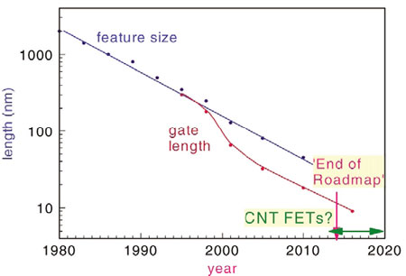 |
| Predicted scaling of feature sizes and gate lengths, according to the International Technology Roadmap for Semiconductors. (Graphic: materialstoday) |
| The feature size is presently 65 nm and the gate length of FETs at this node is 32 nm, which is well within the nano range. This emphasizes how far the conventional top-down fabrication methods of lithography, deposition, and etching can go without asking for a bottom-up approach. But continued scaling is becoming increasingly difficult, so that many firms are researching bottom-up approaches including CNTs as an option. |
| But will they work and what is required for them to be successful? Researchers indicate that nanotubes and semiconductor nanowires could be of interest from 2012 onwards. One thing in favor of nanotubes is that many new materials other than Si and SiO2 are being introduced into integrated circuits, and the previously conservative outlook of the industry to new materials is changing. |
| This article reviews where carbon nanotubes could contribute to microelectronics in terms of vias, interconnects, FETs, and memory elements. It focuses particularly on the requirements this places on the growth of nanotubes. This is not just on forming semiconducting or metallic tubes, but also on controlling growth location and achieving high enough nucleation densities. These barriers to implementation may lead to more pessimistic time scales. |
| Source: materialstoday |

