| Nov 14, 2011 |
Oxide electronics: Electrons in a tight spot |
| (Nanowerk News) Oxide materials are undergoing a renewal of interest from scientists. Poor material quality had, in the past, masked any interesting physics that may have been displayed by these materials, but recent improvements in oxide growth techniques have opened the door to a wide range of novel physical phenomena involving long-range correlations between electrons. Understanding the physics underlying these behaviors will be key to harnessing these effects in electronic devices. |
| Harold Hwang and colleagues from the University of Tokyo in Japan and Stanford University in the US have now completed a detailed study of the electronic behavior of thin layers of the oxide strontium titanate ("Fermi Surface and Superconductivity in Low-Density High-Mobility δ-Doped SrTiO3"). |
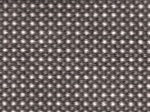 |
| A transmission electron microscopy image of strontium titanate. Bright spots are strontium atoms, and darker spots are titanium atoms. |
| Strontium titanate was once associated with the fabrication of artificial diamond, but it is fast becoming an important material for oxide electronics. In very thin films of various materials, the free motion of electrons becomes confined to just two dimensions, resulting in electronic properties very different from those of the three-dimensional bulk. In the case of strontium titanate (see image), thin layers are known to undergo a transition to a two-dimensional superconducting state at low temperatures. Yet the details of the electronic structure of this intriguing two-dimensional system material had remained a mystery. |
| Hwang and his colleagues studied strontium titanate 'doped' with niobium as a function of the layer thickness and applied magnetic field. The addition of small densities of niobium atoms in a narrow region, a process known as delta-doping, aids the creation of the two-dimensional electronic state by ensuring that the electrons are electrostatically confined in a narrow plane. The team's study of the low-temperature resistance of samples with layer thicknesses of 11–292 nm provided detailed information about the effective mass and mobility of the electrons confined to the layer. The results also highlighted a clear change in the superconducting transition temperature with layer thickness and the existence of both two- and three-dimensional superconductor states. |
| The findings provide concrete information that could now be used in the design of oxide electronics. "We are now at a stage where we can control the electronic structure of this complicated material in much the same way as can be achieved with semiconductors," says Hwang. |
| Source: Tokyo Institute of Technology |

