| Nov 30, 2011 |
Researchers demonstrate fully printed carbon nanotube transistor circuits for displays
|
|
(Nanowerk News) Since the invention of liquid crystal displays in the mid-1960s, display electronics have undergone rapid transformation. Recently developed organic light-emitting diodes (OLEDs) have shown several advantages over LCDs, including their light weight, flexibility, wide viewing angles, improved brightness, high power efficiency and quick response.
|
|
OLED-based displays are now used in cell phones, digital cameras and other portable devices. But developing a lower-cost method for mass-producing such displays has been complicated by the difficulties of incorporating thin-film transistors that use amorphous silicon and polysilicon into the production process.
|
|
Now, researchers from Aneeve Nanotechnologies, a startup company at UCLA's on-campus technology incubator at the California NanoSystems Institute (CNSI), have used low-cost ink-jet printing to fabricate the first circuits composed of fully printed back-gated and top-gated carbon nanotube–based electronics for use with OLED displays. The research was published this month in the journal Nano Letters ("Fully Printed Separated Carbon Nanotube Thin Film Transistor Circuits and Its Application in Organic Light Emitting Diode Control").
|
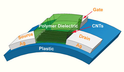 |
| Ink-jet-printed circuit.
|
|
The startup includes collaborators from the departments of materials science and electrical engineering at the UCLA Henry Samueli School of Engineering and Applied Science and the department of electrical engineering at the University of Southern California.
|
|
In this innovative study, the team made carbon nanotube thin-film transistors with high mobility and a high on–off ratio, completely based on ink-jet printing. They demonstrated the first fully printed single-pixel OLED control circuits, and their fully printed thin-film circuits showed significant performance advantages over traditional organic-based printed electronics.
|
|
"This is the first practical demonstration of carbon nanotube–based printed circuits for display backplane applications," said Kos Galatsis, an associate adjunct professor of materials science at UCLA Engineering and a co-founder of Aneeve. "We have demonstrated carbon nanotubes' viable candidacy as a competing technology alongside amorphous silicon and metal-oxide semiconductor solution as a low-cost and scalable backplane option."
|
|
This distinct process utilizes an ink-jet printing method that eliminates the need for expensive vacuum equipment and lends itself to scalable manufacturing and roll-to-roll printing. The team solved many material integration problems, developed new cleaning processes and created new methods for negotiating nano-based ink solutions.
|
|
For active-matrix OLED applications, the printed carbon nanotube transistors will be fully integrated with OLED arrays, the researchers said. The encapsulation technology developed for OLEDs will also keep the carbon nanotube transistors well protected, as the organics in OLEDs are very sensitive to oxygen and moisture.
|
|
The technology incubator at the CNSI was established two years ago to nurture early-stage research and to help speed the commercial translation of technologies developed at UCLA. Aneeve Nanotechnologies LLC has been conducting proof-of-concept work at the tech incubator with the mission of developing superior, low-cost, high-performance electronics using nanotechnology solutions that bridge the gap between emerging and traditional platforms.
|

