| Jan 13, 2012 |
Scientists harness optical tornadoes on a nanochip for sensing and energy applications |
| (Nanowerk News) Boston University researchers demonstrated a new way to efficiently trap and enhance light in nanoscale structures and nanopatterned thin films, which can significantly improve performance of photonic and electronic devices such as nanosensors, thin-film organic solar cells and optical nanochips. |
| Nanoscale light focusing can be achieved by converting free photons into localized charge-density oscillations (surface plasmons) on noble-metal nanostructures, which serve as nanoscale analogs of radioantennas and are typically designed by using antenna theory concepts. Despite offering technological innovation in biosensing and THz metamaterials design, plasmonics faces fundamental physical limitation in the visible frequency band due to high absorptive losses of metals. |
| To address this limitation of plasmonics, the Boston University research team introduced an alternative hydrodynamics-inspired approach for plasmonic nanocircuit engineering, based on trapping incoming light into nanoscale optical tornadoes – areas of circular motion of light flux – 'pinned' to plasmonic nanostructures. They show that creating optical vortices in nanostructures and coupling them into transmission-like sequences results in dramatic optical effects, including optical spectra shaping and orders-of-magnitude increase in the field intensity and quality factors of trapped optical modes. |
 |
| Unlike conventional plasmonic energy harvesting devices based on light scattering, enhancement or guiding, the new hydrodynamics-inspired light trapping platform circulates energy flow through nanoscale optical vortices 'pinned' to plasmonic nanostructures. |
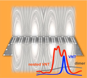
| "We build our design approach around the hydrodynamic analogy of the 'photon fluid,' whose kinetic energy can be locally increased via convective acceleration in the vortex velocity field and then converted into pressure energy to generate localized areas of high field intensity," explained Dr. Svetlana Boriskina, the first author on the paper "Molding the flow of light on the nanoscale: from vortex nanogears to phase-operated plasmonic machinery", which appears in the Jan 2012 issue of the journal Nanoscale. Just as mechanical and hydrodynamic transmissions form a basis of complex machinery, rationally designed nanostructures that trap optical vortices can be combined into complex plasmonic networks enabling nanoscale light routing and switching. |
| The scientists anticipate that their findings are going to drastically change the approach to the engineering of plasmonic nanocircuits, leading to better fundamental insight and novel device solutions in light generation, harvesting and processing. In particular, they demonstrated the advantages of their approach by developing a new platform for surface enhanced Raman spectroscopy, presented in a paper appearing in the journal Nano Letters - "Electromagnetic Field Enhancement and Spectrum Shaping through Plasmonically Integrated Optical Vortices". |
| Moving forward, the scientists are exploring the advantages of the new engineering concept for renewable energy generation, as it helps to eliminate the mismatch between the electronic and photonic length scales in thin-film photovoltaic devices. They expect that the solar energy harvesting platforms designed in the frame of the proposed methodology will help to minimize the thickness of semiconductor needed to absorb light completely, will amplify the signal via plasmonic enhancement mechanism, and will be compatible for integration with either silicon electronics or flexible substrates such as those based on organic and polymer materials. |
| Source: Boston University |

