| Feb 22, 2012 |
New technique creates free-standing piezoelectric ferroelectric nanostructures
|
|
(Nanowerk News) Researchers have developed a "soft template infiltration" technique for fabricating free-standing piezoelectrically active ferroelectric nanotubes and other nanostructures from PZT – a material that is attractive because of its large piezoelectric response. Developed at the Georgia Institute of Technology, the technique allows fabrication of ferroelectric nanostructures with user-defined shapes, location and pattern variation across the same substrate.
|
|
The resulting structures, which are 100 to 200 nanometers in outer diameter with thickness ranging from 5 to 25 nanometers, show a piezoelectric response comparable to that of PZT thin films of much larger dimensions. The technique could ultimately lead to production of actively-tunable photonic and phononic crystals, terahertz emitters, energy harvesters, micromotors, micropumps and nanoelectromechanical sensors, actuators and transducers – all made from the PZT material.
|
|
Using a novel characterization technique developed at Oak Ridge National Laboratory, the researchers for the first time made high-accuracy in-situ measurements of the nanoscale piezoelectric properties of the structures.
|
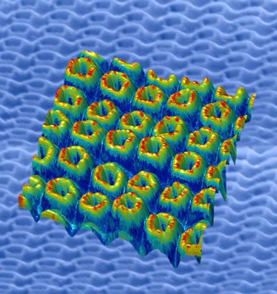 |
| Ferroelectric structures.
|
|
"We are using a new nano-manufacturing method for creating three-dimensional nanostructures with high aspect ratios in ferroelectric materials that have attractive piezoelectric properties," said Nazanin Bassiri-Gharb, an assistant professor in Georgia Tech's Woodruff School of Mechanical Engineering. "We also leveraged a new characterization method available through Oak Ridge to study the piezoelectric response of these nanostructures on the substrate where they were produced."
|
|
The research was published online on Jan. 26, 2012, and is scheduled for publication in the print edition (Vol. 24, Issue 9) of the journal Advanced Materials ("Free-Standing Ferroelectric Nanotubes Processed via Soft-Template Infiltration"). The research was supported by Georgia Tech new faculty startup funds.
|
|
Ferroelectric materials at the nanometer scale are promising for a wide range of applications, but processing them into useful devices has proven challenging – despite success at producing such devices at the micrometer scale. Top-down manufacturing techniques, such as focused ion beam milling, allow accurate definition of devices at the nanometer scale, but the process can induce surface damage that degrades the ferroelectric and piezoelectric properties that make the material interesting.
|
|
Until now, bottom-up fabrication techniques have been unable to produce structures with both high aspect ratios and precise control over location. The technique reported by the Georgia Tech researchers allows production of nanotubes made from PZT (PbZr0.52Ti0.48O3) with aspect ratios of up to 5 to 1.
|
|
"This technique gives us a degree of control over the three-dimensional process that we've not had before," said Bassiri-Gharb. "When we did the characterization, we saw a size effect that until now had been observed only in thin films of this material at much larger size scales."
|
|
The ferroelectric nanotubes are especially interesting because their properties – including size, shape, optical responses and dielectric characteristics – can be controlled by external forces even after they are fabricated.
|
|
"These are truly smart materials, which means they respond to external stimuli such as applied electric fields, thermal fields or stress fields," said Bassiri-Gharb. "You can tune them to behave differently. Devices made from these materials could be fine tuned to respond to a different wavelength or to emit at a different wavelength during operation."
|
|
For example, the piezoelectric effect could permit fabrication of "nano-muscle" tubes that would act as tiny pumps when an electric field is applied to them. The fields could also be used to tune the properties of photonic crystals, or to create structures whose size can be altered slightly to absorb electromagnetic energy of different wavelengths.
|
|
In fabricating the nanotubes, Bassiri-Gharb and graduate student Ashley Bernal (currently an assistant professor at the Rose-Hulman Institute of Technology) began with a silicon substrate and spin-coated a negative electron-beam resist material onto it. A template was created using electron-beam lithography, and a thin layer of aluminum oxide was added on top of that using atomic layer deposition.
|
|
Next, the template was immersed under vacuum into an ultrasound bath containing a chemical precursor solution for PZT. The structures were pyrolyzed at 300 degrees Celsius, then annealed in a two-step heat treating process at 600 and 800 degrees Celsius to crystallize the material and decompose the polymer substrate. The process produced free-standing PZT nanotubes connected by a thin layer of the original aluminum oxide. Increasing the amount of chemical infiltration allows production of solid nanorods or nanowires instead of hollow nanotubes.
|
|
Though the researchers used electron beam lithography to create the template on which the structures were grown, in principle, many other chemical, optical or mechanical patterning techniques could be used for create the templates, Bassiri-Gharb noted.
|
|
In studies done in collaboration with researchers Sergei Kalinin and Alexander Tselev of the Center for Nanophase Materials Sciences at the Oak Ridge National Laboratory, the devices produced by the soft template process were analyzed with band-excitation piezoresponse force microscopy (BPFM). The technique allowed researchers to isolate properties of the AFM tip from those of the PZT sample, allowing analysis in sufficient detail to detect the size-scale piezoelectric effects.
|
|
"One of our most important observations is that these piezoelectric nanomaterials allow us to generate a factor of four to six increase in the extrinsic piezoelectric response compared to the use of thin films," said Baassiri-Gharb. "This would be a huge advantage in terms of manufacturing because it means we could get the same response from much smaller structures than we would have had to otherwise use."
|

