| Posted: September 3, 2007 |
Nanotechnology microscope for ultrafast processes |
|
(Nanowerk) International team of scientists proposes new ultramicroscope for nanostructures, allowing for the direct and non-invasive measurement of ultrafast processes on attosecond timescales with high spatial and temporal resolution.
|
|
Metallic nanostructures, consisting of a few thousand atoms, exhibit optical and electronic properties which are not present in extended solid state systems. The interaction of electromagnetic radiation (light) with nanoparticles leads to collective, coherent oscillations of electrons (so called surface plasmons). A team of scientists from the Georgia State University (Atlanta, Georgia, USA), the Max Planck Institute of Quantum Optics in Garching (MPQ), and the Ludwig Maximilians University at Munich (LMU) have now proposed a new microscope that allows for the first time to resolve the ultrafast dynamics of plasmonic fields with high spatial and temporal resolution ("Attosecond nanoplasmonic-field microscope").
|
|
In particular, applications in optical and optoelectronical information processing, transfer, and storage would benefit from a better understanding of these collective excitations. Furthermore, this ultramicroscope would have nanotechnology applications in the spectroscopy of single (bio)-molecules, where nanoparticles act as antennas for light interaction.
|
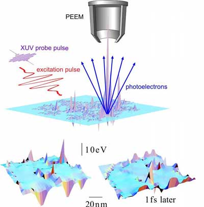 |
Principle of the nano-microscope for ultrafast processes. (Image: CAS)
|
|
Without deeper insight, the makers of colored glass vases in ancient Rome or church windows in the middle ages have already used the properties of metallic nanoparticles to their advantage. The shiny red color was achieved by adding gold dust to the glass melt. The origin of this effect is understood by specialists today: nanoparticles, i.e. particles with extensions in the range from a few to 100 nanometers - less than the wavelength of visible light (ca. 400 - 800 nanometers) - consist of as little as a few thousand atoms. If such a particle is exposed to visible light, the freely moving conduction electrons are displaced by the light's electric field. Since the structure is small, they are not moving very far, but alternate being bunched on one side or the other. This way, the electrons are moving collectively in synchronized coherent oscillations. Such oscillations have particle character and are called surface plasmons. The red color of ancient Roman vases and old church windows is based on the absorption of part of the visible light by the gold nanoparticles, which is converted into plasmons. Then the residual light shines in the complementary colors.
|
|
"Plasmons create very high electromagnetic fields at the nanoparticle and its direct environment. But how these fields are created and how they decay is not understood in detail. The fastest dynamics of the collective motions takes place in only a few hundred attoseconds (1 attosecond is a billionth of a billionth of a second) and belongs therefore to the fastest processes in nature," explains Dr. Matthias Kling, Junior Research Group leader at MPQ.
|
|
A new method to resolve the dynamics of plasmonic fields with the highest temporal and spatial precision has been suggested by the theoretical physicist Prof. Mark Stockman (Georgia State University at Atlanta, Georgia, USA) together with experimental physicists from LMU and MPQ in Germany. In their model (see figure), the scientists simulated a geometric assembly of silver nanoparticles on a surface, which are then excited by an (extremely short) few femtosecond pulse (a femtosecond is a millionth of a billionth of a second). The interaction with the light-pulse -- consisting of only a few oscillation periods -- leads to the formation of plasmonic fields, whose amplitudes and frequencies (between the near infrared and near ultraviolet) depend on the size, shape, and environment of the nanoparticles. The plasmon dynamics is probed by a 170 attosecond, extreme ultraviolet laser pulse incident on the nanosystem that is synchronized with the excitation pulse and releases electrons. The plasmonic fields are monitored by the energy and spatial distribution of these so called photoelectrons as they were - prior to their detection - accelerated by these fields.
|
|
"In our suggested approach we combine two techniques, which are by themselves already state-of-the-art: the photoemission electron microscope, also called PEEM, and the attosecond streak camera," explains Prof. Ulf Kleineberg from LMU. "This way we obtain a spatial resolution, which is on the order of the dimension of the nanoparticles between a few ten to hundred nanometers, and achieve simultaneously -- due to the use of attosecond light flashes -- the extremely high time resolution in the attosecond domain. The measurement principle lays the foundation to measure the formation and temporal evolution of these fields and to control them by specifically shaped laser pulses in the future."
|
|
Generally the nanoplasmonic ultramicroscope would allow for the first direct observation of ultrafast processes in nanosystems, such as the conversion of sunlight into electrical energy. The authors see future applications of the technique particularly in the development of novel devices, in which localized nanoplasmonic fields replace electrons in conventional electronics, i.e. are used for information transfer, processing, and storage. "The advantage would be that plasmons in these nanosystems allow for information processing and transfer at much higher frequencies (ca. 100,000 times) as compared to electrons in solid state systems. This way, extremely fast optoelectronic and optical devices for computations and information processing may be realized."
|

