| May 21, 2012 |
Production of low-defect single-walled carbon nanotubes in large quantities at the Fraunhofer IWS |
| (Nanowerk News) Thanks to public funding by the BMBF (German Federal Ministry of Research and Technology) within the framework of the Carbon Nanotubes Innovation Alliance – CNT, the Fraunhofer IWS Dresden was able to develop a process suitable especially for the mass production of single-walled carbon nanotubes. The single-walled carbon nanotubes are produced inside a reactor during a pulsed arc evaporation of carbon. |
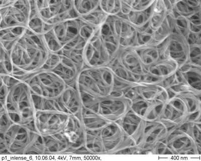 |
| Isotopes mat of nanofibers made of single-walled carbon nanotubes. (© Fraunhofer IWS Dresden) |
| The diameters of the produced carbon nanotubes are between 1.0 and 1.6 nm. This corresponds to about 1 / 10 000 of the human hair. After the production the tube length lies in the range of several micrometers. Carbon nanotubes then show a metallic conductivity or semiconductivity depending on their diameter. The proportion of semiconducting to metallic conducting carbon nanotubes is in general between two thirds and one third. This proportion, however, can be specifically varied with the process developed at the Fraunhofer IWS and is yet another characteristic feature of the process. Moreover, the carbon nanotubes have a very low defect density. So there are hardly any defects with the hexagonal arrangement of the atoms. |
| The Fraunhofer IWS is currently one of the few institutes worldwide which is able to produce the single-walled carbon nanotubes on a kg-scale. The process seems to be very promising for the industrial mass production. It allows for the development of attractive applications based on the excellent electrical, thermal and mechanical properties of the single-walled carbon tubes. |
| In case of the single-walled carbon nanotubes the permissible current density - i.e. the number of charge carriers that may flow through a defined conductor per time unit - is 1000 times higher than that of copper. The thermal conductivity is about 15 times that of copper. The E-module of a single carbon nanotube can be 5 times as high as that of a carbon fibre and its tensile strength can be up to 10 times that of a carbon fibre. Single-walled carbon nanotubes are thus a high-tech material which allows the researchers in Dresden to press ahead with innovative and unique product developments. |
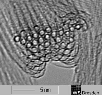 |
| Bundle of carbon nanotubes (Transverse section) (© Fraunhofer IWS Dresden) |
| The research of the Fraunhofer IWS focuses on electronic applications for the single-walled carbon nanotubes. The especially good electric conductivity of the single-walled carbon nanotubes will lead, for example, to a large application potential in photovoltaics as transparent conducting layers. In addition, work is being done on the production of electrically conductive inks based on carbon nanotubes, which can be used to directly print conductive paths with conventional inkjet printers. |
| Market forecasts predict a strong growth of the production of carbon nanotubes. Since research in this area has been done for years, the first products are already on the market – especially in the area of polymer composites for sports equipment. Other product improvements for the use of carbon nanotubes as a composite material in polymer materials are close to being introduced on the market. In connection with the low-cost mass production of single-walled carbon nanotubes, a multitude of new applications are conceivable in the area of actuating elements and sensor technology. |
| The production, functionalization and application of carbon nanotubes is one focus at this year's Nanofair, which will take place between 12 and 13 June in the "Internationale Kongresszentrum Dresden". Experts from 23 countries will present international know how in nano technology. |
| Source: Fraunhofer IWS |

