| Jun 18, 2012 |
Graphene decoupling of organic/inorganic interfaces |
| (Nanowerk News) Cryogenic ultrahigh vacuum scanning tunneling microscopy (STM) was employed by researchers in the Center for Nanoscale Materials' Electronic & Magnetic Materials & Devices Group to uncover exceptionally weak molecule-surface interactions between fullerene C60 deposited onto epitaxially grown graphene on silicon carbide substrates (see paper in Nano Letters: "Structural and Electronic Decoupling of C60 from Epitaxial Graphene on SiC"). |
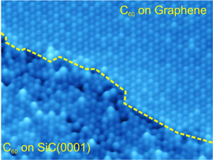 |
| STM three-dimensional rendered image of a C60 self-assembled monolayer at a domain boundary of graphene and bare SiC(0001); each C60 molecule is 1 nm in diameter. |
| The first layer of C60 molecules self-assembles into well-ordered close-packed islands. In situ scanning tunneling spectroscopy reveals a highest occupied molecular orbital–lowest unoccupied molecular orbital gap of 3.5 V, which is close to the value of solid and gas-phase C60. This finding indicates a significantly smaller amount of charge transfer from the C60 to the graphene as compared with C60 adsorbed onto metallic surfaces. |
| Usually interface effects dominate over the properties of adsorbed molecules. Here, however, a perfect two-dimensional material (graphene) has completely decoupled the organic system from the charged interface states of the silicon carbide surface reconstruction. Improving molecule-based organic photovoltaics and biosensors relies on minimal substrate-molecule interaction to preserve intrinsic molecular functionalities, which was achieved in this case via an inert graphene "barrier" layer. |
| Source: Argonne National Laboratory |

