| Mar 01, 2006 |
"Nano Skins" Show Promise as Flexible Electronic Devices
|
|
(Nanowerk News) A team of researchers has developed a new process to make flexible, conducting "nano skins" for a variety of applications, from electronic paper to sensors for detecting chemical and biological agents. The materials, which are described in the Feb. 1, 2006 online issue of the journal Nano Letters in an article titled "Aligned Carbon Nanotube-Polymer Hybrid Architectures for Diverse Flexible Electronic Applications", combine the strength and conductivity of carbon nanotubes with the flexibility of traditional polymers.
|
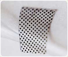 |
| A flexible, conducting "nano skin" with organized arrays of nanotubes embedded throughout. (Photo by Rensselaer/Yung Joon Jung)
|
|
"Researchers have long been interested in making composites of nanotubes and polymers, but it can be difficult to engineer the interfaces between the two materials," says Pulickel Ajayan, the Henry Burlage Professor of Materials Science and Engineering at Rensselaer Polytechnic Institute. "We have found a way to get arrays of nanotubes into a soft polymer matrix without disturbing the shape, size, or alignment of the nanotubes."
|
|
Nanotube arrays typically don’t maintain their shape when transferred because they are held together by weak forces. But the team has developed a new procedure that allows them to grow an array of nanotubes on a separate platform and then fill the array with a soft polymer. When the polymer hardens, it is essentially peeled back from the platform, leaving a flexible skin with organized arrays of nanotubes embedded throughout.
|
|
The skins can be bent, flexed, and rolled up like a scroll, all while maintaining their ability to conduct electricity, which makes them ideal materials for electronic paper and other flexible electronics, according to Ajayan.
|
|
"The general concept — growing nanotubes on a stiff platform in various organizations, and then transferring them to a flexible platform without losing this organization — could have many other applications, all the way from adhesive structures and Velcro-like materials to nanotube interconnects for electronics," says Swastik Kar, a postdoctoral researcher in materials science and engineering at Rensselaer and lead author of the paper, along with Yung Joon Jung, assistant professor of mechanical and industrial engineering at Northeastern University and a recent doctoral student in Ajayan’s Rensselaer lab.
|
|
For example, with researchers at the University of Akron, Ajayan is using a similar process to mimic the agile gecko, with its uncanny ability to run up walls and across ceilings. The team recently reported a process for creating artificial gecko feet with 200 times the sticking power of the real thing, using nanotubes to imitate the thousands of microscopic hairs on a gecko’s footpad. Ajayan’s team is also working with Ali Dhinojwala, associate professor of polymer science at Akron, to develop a range of products with nanotubes and flexible substrates.
|
|
The researchers also envision using the process to build miniature pressure sensors and gas detectors. "There are a lot of possibilities if you have an easy way to transfer the nanotubes to any platform, and that is what we have developed," Ajayan says.
|
|
The team has shown that the flexible materials demonstrate an extremely useful physical property called "field emission." When a voltage is applied to certain materials, electrons are pulled out from the surface, which can be used to produce high-resolution electronic displays. "Nanotubes are very good field emitters because they have a low threshold for emission and they produce high currents," Kar says. "But when you lay nanotubes very close to each other, each tube tends to shield its neighbor from the electric field."
|
|
This effect has limited the development of field emission devices based on densely packed, aligned nanotubes, but it seems to go away when the nanotubes are embedded in a polymer, according to Kar. Tests showed that the team’s "nano skins" are excellent field emitters when compared to some of the best values obtained by other research groups.
|
|
Several other Rensselaer researchers also collaborated on the project, along with colleagues from New Mexico State University. Funding for this research was provided by two National Science Foundation Nanoscale Science and Engineering Centers: Rensselaer’s Center for Directed Assembly of Nanostructures and Northeastern’s Center for High-rate Nanomanufacturing. Additional funding came from the Focus Center-New York, which is part of the Interconnect Focus Center.
|

