| Posted: February 1, 2008 |
Sketching on silicon |
| (Nanowerk News) Silicon is the workhorse material of the semiconductor industry because it is on this element that the integrated circuits of modern microprocessor devices are built. In order to satisfy the ever-increasing speed and power demands of computing, the miniaturization of such electronic components is the focus of much research. |
| So-called top-down methods used to carve ever-smaller features into the surface of silicon wafers will result in performance benefits for a little longer, but there are size limits to which these structures can be practically reduced. An alternative fabrication approach, however, relies upon the bottom-up assembly of molecular building blocks to form nanoscale electronic components. |
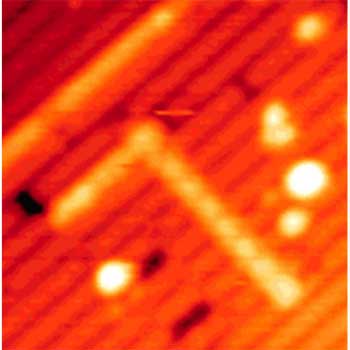 |
| Continuous molecular lines with perpendicular geometries can be drawn on silicon substrates using two different compounds that grow in different directions when they react with the surface atoms. (Reproduced with permission from JACS 129, 12304–12309 (2007). Copyright (2007) the American Chemical Society) |
| Now, Maki Kawai and colleagues from RIKEN’s Discovery Research Institute in Wako, have discovered a way to ‘draw’ perpendicular lines—made from different molecules—on silicon surfaces that comprise pairs of atoms, known as dimers, aligned in parallel rows. Writing in the Journal of the American Chemical Society ("Selective Chain Reaction of Acetone Leading to the Successive Growth of Mutually Perpendicular Molecular Lines on the Si(100)-(2x1)-H Surface"), they found that acetone—a small organic compound—readily forms straight molecular lines along the rows of silicon dimers on these substrates. |
| The silicon substrate was first exposed to atomic hydrogen, resulting in the formation of silicon–hydrogen bonds. A small number of the silicon atoms do not react, however, and these so-called ‘dangling-bond sites’ are quite reactive and can form bonds with organic molecules. When an acetone molecule becomes fixed to the surface by reacting with a dangling-bond site, a new dangling-bond site is created in the adjacent silicon dimer in the row, setting off a chain reaction in which more acetone molecules bond to the surface to form a molecular line. |
| Kawai and co-workers went on to show that acetone lines can be grown from the ends of lines formed from other molecules on the same silicon surface. In contrast with acetone, molecules of a compound called allylmercaptan form lines in a direction perpendicular to the rows of silicon dimmers (see figure above). In this way, mutually perpendicular lines can be formed on these silicon surfaces, since their direction can be simply controlled by changing the gas feed to the surface. |
| Because dangling-bond sites can also be produced at predefined positions on the surface with a scanning tunneling microscope, the origin of the lines can be precisely controlled. The ability to form molecular arrays with carefully controlled geometries on a material around which the semiconductor industry revolves could have significant implications for the rapidly developing field of molecular electronics. |
| Source: Riken |

