| Posted: June 12, 2008 |
AIST makes transistor with semiconductor carbon nanotube |
|
(Nanowerk News) Japan's National Institute of Advanced Industrial Science and Technology (AIST) announced that it developed a transistor with highly purified semiconductor single-wall carbon nanotubes (SWCNT).
|
|
The transistor has an On/Off ratio (ratio between on-state and off-state of drain current) of 1×10⁵ or higher and a carrier mobility of 2cm2/Vs or higher.
|
|
AIST developed a technology to fabricate a high-concentration SWCNT and used it in the production of transistor. First, powders of commercially available SWCNT material were dispersed in a solution by using polyfluorene (PFO), which is a conjugated polymer, as a dispersing agent. Then, the mixed dispersion solution was separated by using an ultracentrifuge at a rotation of 30,000rpm or faster so that the supernatant solution of semiconductor SWCNT thus separated was selectively extracted.
|
|
After removing PFO, a semiconductor SWCNT film was formed by coating a substrate with the semiconductor SWCNT solution.
|
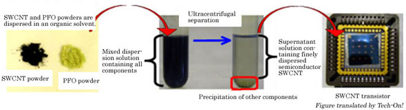 |
| The process of SWCNT dispersion and ultracentrifugal separation, and SWCNT transistor.
|
|
A transistor using a SWCNT thin film is less expensive, superior in mass productivity and highly suitable for a larger surface area. Transistor performance degrades significantly, however, if a metal SWCNT other than the semiconductor SWCNT or even a small amount of a metallic impurity gets mixed in. As a result, there has been strong demand for the development of a technology for separating and extracting high-purity semiconductor SWCNT, according to AIST.
|
|
In order to obtain a high-quality semiconductor SWCNT thin film, ultracentrifugal separation was conducted for 60 minutes. As a result, a metal SWCNT and other impurities were removed so that their remaining amount became less than the detection limit. PFO remaining in the semiconductor SWCNT dispersion solution after ultracentrifugal separation was also removed, according to AIST. Then, filtration, cleansing and heating treatment were carried out.
|
|
Moreover, AIST reportedly evaluated the preferable conditions for film thickness reduction based on spin coating, etc.
|
|
To improve the transistor characteristics, a technique called "dielectrophoresis" was used for thin film formation so that SWCNTs facing in different directions were oriented in one direction simultaneously with the reduction of film thickness. Specifically, the semiconductor SWCNT dispersion solution was dropped on an electrode pair prepared in advance, and the solvent was evaporated while applying the alternating electric field between the electrodes, AIST said.
|
|
With this technique, the SWCNTs were concentrated between the electrodes, while at the same time they were oriented in the direction of the electric field, according to AIST.
|
|
The achievement was published in the June 9, 2008, online edition of Applied Physics Letters.
|

