| Posted: September 17, 2008 |
Light and electrons cooperate in single nanostructure |
|
(Nanowerk News) Light hitting a surface creates very different kinds of disturbances depending on whether it's a metal or a semiconductor. But combining these two materials in a single nanostructure could lead to devices that benefit from the best properties of each. In order to better understand how this might work, researchers reporting in the September 12, Physical Review Letters have now characterized the coupling between excitons – excited electron states in semiconductors – and plasmons, which exist in metals. Understanding the details of the plasmon-exciton interaction might help researchers develop optical computers, plasmon lasers, or improved solar cells ("Coherent Exciton–Surface-Plasmon-Polariton Interaction in Hybrid Metal-Semiconductor Nanostructures").
|
|
When light hits a metal, it can create a surface plasmon polariton--often called simply a "surface plasmon"--which is a traveling wave combining electromagnetic fields with electron oscillations. Researchers are using tiny plasmon antennas to funnel more light into solar cells (photovoltaics), increasing their efficiency. Others studying "plasmonics" hope to develop devices that replace some electric currents with plasmon waves, because plasmons can theoretically carry as much information as light pulses but squeeze it into the nanometer-sized wires used in standard computer chips.
|
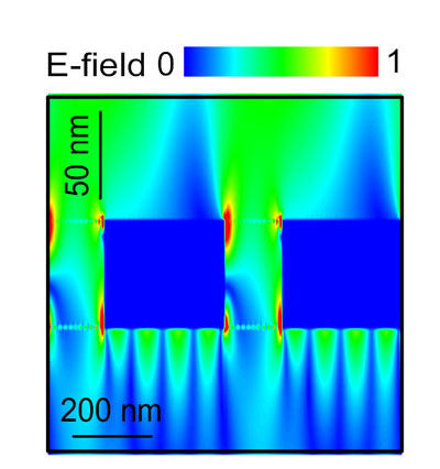 |
| Golden waves. This computer simulation shows the strength of the electric field surrounding nanoscale gold strips (shown in cross section) hit with infrared light from above. In experiments, researchers measured the interactions of the gold's surface plasmons--waves of electromagnetic fields and electrons--with electrons (excitons) in the semiconductor slab below (not shown). (Image: American Physical Society)
|
|
The emerging field of plasmonics suffers, however, from the fact that plasmons survive for only 10 to 100 femtoseconds before they decay into normal light waves or simply transform into vibrations of atoms. "The big challenge is to overcome these losses," says Christoph Lienau of Carl von Ossietzky University in Oldenburg, Germany. One solution would be to amplify the plasmon signal by feeding it photons emitted by a semiconductor touching the metal. A light pulse could excite a semiconductor electron into a state called an exciton, which would then drop back down to the ground state and emit the photon. But to build such an amplifier, Lienau says, you need to know how excitons and plasmons "talk to each other." Others have observed this interaction through changes in the optical properties of semiconductors coupled to metal nanostructures, but no one has been able to precisely measure the way energy transfers between the two materials.
|
|
To study plasmon-exciton interactions, Lienau and his colleagues designed a "hybrid" nanostructure whose plasmons could be precisely controlled. They started with a 10-nanometer thick slice of the semiconductor gallium arsenide and then laid several parallel gold strips on top, each 360 nanometers wide, leaving 140-nanometer gaps between them. The team shined an infrared laser onto the strips and measured how much of the light was reflected. From decreases in this reflection, they could tell that some of the light was converted into plasmons on the top and bottom surfaces of the gold strips. By varying the angle of the incoming laser beam, the team could change the wavelength of these plasmons. When they tuned this wavelength to near the exciton resonance in the gallium arsenide at 810 nanometers, they detected an even further decrease in reflected light. The implication was that the plasmons at the bottom of the strips were interacting with excitons in the semiconductor.
|
|
The team then constructed a mathematical model of coupled oscillators to explain their data. From this, they calculated the exciton-plasmon coupling strength to be 8 millielectron volts, which implies that it takes roughly 250 femtoseconds for a plasmon to transform into an exciton. This conversion time could be shortened by a factor of 5 or so by optimizing the device, but in general, all hybrid structures will have this basic coupling, Lienau says.
|
|
"The work is beautiful in both its scientific detail and thoroughness and also in its potential impact," says Kobus Kuipers of the FOM Institute for Atomic and Molecular Physics (AMOLF) in Amsterdam. Although this system essentially converts plasmons into excitons, it could run the other way if an electric current or second laser pumped excitons into the semiconductor. So Kuipers says this detailed study will directly benefit those working to amplify plasmon signals for devices as well as researchers developing a plasmon laser, sometimes called a SPASER.
|

