| Posted: November 5, 2008 |
Light my photonic crystal |
|
(Nanowerk News) "Circuits of light" are the dream. Researchers hope photonic chips will someday process light signals faster than today's chips can handle electronic ones and zeros. In the Rapid Communications section of the October Physical Review E, researchers describe a method for adding light-emitting elements in a precise way to a future photonic circuit ("Local nanofluidic light sources in silicon photonic crystal microcavities"). They filled a small hole in a silicon wafer with tiny chunks of fluorescent semiconductor and imaged the pattern of light that was generated. The technique permits easy removal and replacement of the particles and offers a way of creating photonic structures that include light emitters set out in some desired pattern.
|
|
Photonic structures usually start with a solid containing an array of tiny holes or voids. Some of the holes are then filled in, enlarged, or otherwise modified in order to make waveguides, resonators, or other elements that can manipulate light. To add luminous particles to the photonic toolbox, researchers have recently tried immersing photonic materials in fluids containing quantum dots--fluorescent semiconductor particles with nanometer diameters. Although the dots have been shown to modify the electromagnetic properties of the structure, this method affords no control over the placement of the dots.
|
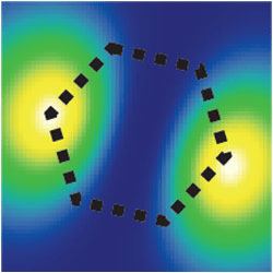 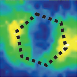 |
| Photonic beacon. Calculations of the electric field intensity produced by quantum dots filling a cavity in a photonic structure, viewed looking down on the structure (top), compared with the experimental data (bottom). A new technique allows these fluorescent particles to be precisely placed in a tiny volume.
|
|
In previous research, Diederik Wiersma of the European Laboratory for Non-linear Spectroscopy (LENS) in Florence, Italy, and his colleagues showed how to use an ultrasmall pipette in conjunction with observation by microscope to deposit less than one femtoliter of a liquid into correspondingly small pores in solids ("Rewritable photonic circuits"). They have now used this technique to fill a hole in a silicon photonic structure with a drop of toluene containing a few thousand, roughly 3-nanometer-diameter, lead-sulfide quantum dots.
|
|
Their photonic structure was a 260-nanometer-thick silicon wafer perforated by a honeycomb pattern of 210-nanometer-diameter holes. This two-dimensional photonic crystal had a larger central cavity, 635 nanometers across, replacing seven normal-sized holes. The researchers calculated that this structure would cause the central cavity to have a strong interaction--a resonance--with light having a wavelength near 1300 nanometers, close to the emission wavelength of the quantum dots.
|
|
The team filled the cavity with quantum dots in toluene and then used longer-wavelength light to excite the dots. They then measured the emission pattern across the cavity by means of a scanning near-field optical microscope (SNOM). The spectrum of quantum dots alone displays a broad emission peak centered at just over 1300 nanometers. But the emission from the dot-filled cavity had a very sharp peak, corresponding to the cavity resonance, at 1315 nanometers, along with a broader peak at a shorter wavelength. Moreover, the relative intensity of the sharp and the broad peak varied from the center to the edges of the cavity in a way that matched the team's calculations for the expected field profile. A sharp peak means a strong resonance, indicating that the quantum dot emissions interacted strongly with the photonic structure--an important step for creating functional devices combining these ingredients.
|
|
"I like the local injection technique," says Dirk Englund of Stanford University, adding that SNOM is a great way to assess how uniformly the quantum dots distribute themselves in the cavity.
|
|
When confined in the cavity, toluene doesn't evaporate because of surface tension; a filled cavity remains stable for more than a month, says team member Francesca Intonti of LENS. However, the quantum dots can be easily removed by washing the silicon structure with ethanol and drying it in an oven. That makes the technique ideal for experimenting with the placement of quantum dots in a more complex structure, perhaps with multiple cavities, says Intonti. The ability to "write" a light-emitting pattern could be especially useful for creating photonic circuits that are part of systems for communicating information optically, says team member Silvia Vignolini, also of LENS.
|

