| Sep 24, 2012 |
Researchers demonstrate 'giant' forces in super-strong nanomaterials
|
|
(Nanowerk News) In a study that could lead to advances in the emerging fields of optical computing and nanomaterials, researchers at Missouri University of Science and Technology report that a new class of nanoscale slot waveguides pack 100 to 1,000 times more transverse optical force than conventional silicon slot waveguides
|
|
The findings could lead to advances in developing optical computers, sensors or lasers, say researchers Dr. Jie Gao and Dr. Xiaodong Yang, both assistant professors of mechanical engineering at Missouri S&T.
|
|
In their research article, published in the Sept. 24 issue of Optics Express ("Giant transverse optical forces in nanoscale slot waveguides of hyperbolic metamaterials"), Gao and Yang describe the unusual optical and mechanical properties of nanometer-scale metal-dielectric structures called metamaterials. The researchers created computer simulations of nanometer-scale models of metamaterial slot waveguides, which are structures designed to channel beams of light from one area to another. Waveguides function like tiny filaments or the wires of an integrated circuit, but on a much smaller scale.
|
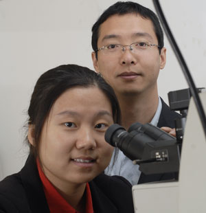 |
| Dr. Jie Gao (foreground) and Dr. Xiaodong Yang, both assistant professors of mechanical engineering at Missouri University of Science and Technology, report that a new class of nanoscale slot waveguides pack 100 to 1,000 times more transverse optical force than conventional silicon slot waveguides.
|
|
For their study, the Missouri S&T researchers simulated slot waveguides made of layered structures of a metal (in this case, silver) and a dielectric material (germanium), arranged like the alternating bread and meat in a club sandwich. A nanometer – visible only with the aid of a high-power electron microscope – is one billionth of a meter, and some nanomaterials are only a few atoms in size.
|
|
Gao and Yang simulated what would happen with modeled identical waveguides – each 40 nanometers wide and 30 nanometers tall – that were stacked with a tiny air gap between them. They then measured the transverse optical force between the two waveguides. Optical force refers to the way beams of light can be made to attract or repel each other, as magnets do.
|
|
In their experiments on the simulated metamaterials, the Missouri S&T researchers found that “the transverse optical forces in slot waveguides of hyperbolic metamaterials can be over two orders of magnitude stronger than that in conventional dielectric slot waveguides.”
|
|
“The calculation on realistic metal-dielectric multilayer structures indicates that the predicted giant optical forces are achievable in experiments,” the researchers explain in their Optics Express article. They add that their finding “will open the door for various optomechanical applications in nanoscale, such as optical nanoelectromechanical systems, optical sensors and actuators.”
|
|
By experimenting with materials at the nanometer level, researchers often find that even common materials exhibit unusual properties. For example, metals developed at the nanometer scale may have fewer defects and could lead to stronger materials for construction. Semiconductors and magnetic materials developed at the nanometer scale may have different properties than the bulk material.
|
|
The team also recently described the optical properties of a single metamaterial waveguide in the Journal of the Optical Society of America ("Nanoscale metamaterial optical waveguides with ultrahigh refractive indices").
|
|
Earlier this year, Yang was the lead author of an article published in Nature Photonics that described how nanoscale three-dimensional optical cavities made from metamaterials can generate the most powerful nanolaser beams to date. The Nature Photonics paper described how this new class of optical cavities holds promise for other technologies, including photonic integrated circuits, LEDs, quantum optics, nonlinear optics and optical sensing.
|
|
Gao and Yang plan to move their research from modeling and simulation to actual fabrication of metamaterials. Working with the Materials Research Center at Missouri S&T, the two are able to use a focused ion beam (FIB) scanning electron microscope to modify materials being analyzed. But the two also hope to develop a nanofabrication facility at Missouri S&T.
|

