| Oct 05, 2012 |
Silicon at the breaking point as basis for more-efficient transistors
|
|
(Nanowerk News) Stretching a layer of silicon can build up internal mechanical strain which can considerably improve its electronic properties. With strained silicon, one can, for example, build faster and less power-consuming microprocessors. Researchers at the Paul Scherrer Institute and the ETH Zurich have developed a method which allows them to produce 30-nanometer-thick highly strained wires in a silicon layer. This strain is the highest that has ever been observed in a material which can serve as the basis for electronic components. The aim is to produce high-performance and low-power transistors for microprocessors based on such wires. As a starting point, the method uses a substrate with a silicon layer that is already under low strain. By selectively etching away the surrounding material, a thin wire is produced in the silicon layer which hangs like a tiny bridge over a gorge, with the highest strain concentrated at its narrowest point. The researchers report their results in the latest issue of the online journal Nature Communications ("Top-down fabricated silicon nanowires under tensile elastic strain up to 4.5%").
|
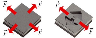 |
| The principle of the method used for achieving a high stress in silicon. Firstly, the forces act in all directions in the silicon layer. If small parts of the layer are then etched away to create a thin wire, the forces act along the wires so that a high stress is created within them. (Graphics: Paul Scherrer Institut/ R. Minamisawa)
|
|
The principle of the method used for achieving a high stress in silicon. Firstly, the forces act in all directions in the silicon layer. If small parts of the layer are then etched away to create a thin wire, the forces act along the wires so that a high stress is created within them. (Graphics: Paul Scherrer Institut/ R. Minamisawa)
|
|
There are limited possibilities for increasing the efficiency of microprocessors based on silicon technology by decreasing the size of individual building elements. But there are other promising ways, which are to some extent already used by industry, such as stretching or compressing silicon, thereby creating mechanical tension that helps to improve the electronic properties of the material. For example, tension in the correct direction significantly increases the mobility of electrons, which makes transistors much faster switching elements. "There is actually no magic behind building up tension in a wire - you just have to pull strongly on both ends", explains Hans Sigg of the Laboratory for Micro- and Nanotechnology at the Paul Scherrer Institute. "The challenge is to implement such a wire in a stressed state into an electronic component."
|
|
30-nm–wide Silicon Bridge
|
|
Researchers at the Paul Scherrer Institute have now developed a method to create silicon wires which are tightly connected to their surrounding material and are under a tension which is more than twice as high as that used in contemporary components. As the initial material, they have used an industrially produced substrate with a slightly stressed silicon layer fixed onto a buried silicon oxide layer. "It was important for us to show that our method is compatible with the fabrication methods and materials of industry", says Hans Sigg. "You can imagine the material as being pulled in all directions before it is attached to the oxide sublayer", explains Renato Minamisawa from the Paul Scherrer Institute, who conducted the experiments along with Martin Süess from ETH Zürich. "The substrate then holds the layer in place so that it cannot contract anymore."
|
|
In the process, cleverly chosen parts of the silicon layer and the oxide sublayer are removed by the respective etchants, to create a thin wire from the silicon layer – 30 nanometers wide and 15 nanometers thick – that is attached to the rest of the material only at its endpoints. The method is exemplary for the possibilities of modern nanotechnology. In this way, thousands of such wires can be accurately produced in a well-defined stressed state. Thus the method is very reliable. "And it is even scalable, meaning that the wires can be fabricated as small as you want", Sigg points out.
|
|
Faster Transistors through high Stresses
|
|
"Since all the force which was distributed over a larger area before the etching now has to concentrate in the wire, a high tension is created within it", says Minamisawa, "the strongest tension ever generated in silicon; probably even the strongest obtainable before the material breaks." Raman spectroscopy and computer simulation were conducted in the Laboratory for Nanometallurgy under Ralph Spolenak at the ETH, in order to measure the stress distribution in detail. In the future, such wires will also be studied at the Swiss Light Source (SLS) at the Paul Scherrer Institute. The objective of such experiments will especially be to determine how much the electronic properties of the material have changed.
|
|
The ultimate goal would be to use these silicon nanowires as fast transistors within microprocessors. To achieve this, the researchers will now investigate, with partners, how to embed these wires in a transistor structure. For that purpose, the wires need to be "doped", i.e. provided with small amounts of atoms of other elements, "wrapped up" in a thin oxide and provided with metal contacts. "But even if they do not end up in microelectronic applications, our research could show what the limits of silicon electronics really are," explains Minamisawa.
|
|
The project has been supported by the Swiss National Science Foundation and the Swiss Priority Program nano-tera.ch.
|

