| Mar 22, 2013 |
Scientists discover new nanotechnology technique to charge memory chips |
| (Nanowerk News) IBM today announced a materials science breakthrough at the atomic level that could pave the way for a new class of non-volatile memory and logic chips that would use less power than today’s silicon based devices. Rather than using conventional electrical means that operate today’s semiconducting devices, IBM’s scientists discovered a new way to operate chips using tiny ionic currents, which are streams of charged atoms that could mimic the event-driven way in which the human brain operates. |
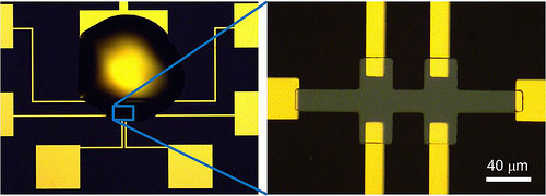 |
| Optical image of a typical ionic liquid (IL) gated device with a droplet of IL on top of the gate electrode and the oxide channel. The gold squares are pads used to make contact to the device via wire-bonding. On right is the magnified image of the device showing the channel (brownish yellow) and the gold electrical contacts (bright yellow). The contacts on the right and left of the channel are the source and drain contacts. The four other contact are used for 4-wire resistance & Hall measurements. (Credit: IBM) |
| Today’s computers typically use semiconductors made with CMOS process technologies and it was long thought that these chips would double in performance and decrease in size and cost every two years. But the materials and techniques to develop and build CMOS chips are rapidly approaching physical and performance limitations and new solutions may soon be needed to develop high performance and low-power devices. |
| IBM research scientists showed that it is possible to reversibly transform metal oxides between insulating and conductive states by the insertion and removal of oxygen ions driven by electric fields at oxide-liquid interfaces. Once the oxide materials, which are innately insulating, are transformed into a conducting state, the IBM experiments showed that the materials maintain a stable metallic state even when power to the device is removed. This non-volatile property means that chips using devices that operate using this novel phenomenon could be used to store and transport data in a more efficient, event-driven manner instead of requiring the state of the devices to be maintained by constant electrical currents. |
| “Our ability to understand and control matter at atomic scale dimensions allows us to engineer new materials and devices that operate on entirely different principles than the silicon based information technologies of today,” said Dr. Stuart Parkin, an IBM Fellow at IBM Research. “Going beyond today’s charge-based devices to those that use miniscule ionic currents to reversibly control the state of matter has the potential for new types of mobile devices. Using these devices and concepts in novel three-dimensional architectures could prevent the information technology industry from hitting a technology brick wall.” |
| To achieve this breakthrough, IBM researchers applied a positively charged ionic liquid electrolyte to an insulating oxide material - vanadium dioxide - and successfully converted the material to a metallic state. The material held its metallic state until a negatively charged ionic liquid electrolyte was applied, to convert it back to its original, insulating state. |
| Such metal to insulator transition materials have been extensively researched for a number of years. However, contrary to earlier conclusions, IBM discovered that it is the removal and injection of oxygen into the metal oxides that is responsible for the changes in state of the oxide material when subjected to intense electric fields. |
| The transition from a conducting state to an insulating state has also previously been obtained by changing the temperature or applying an external stress, both of which do not lend themselves to device applications. |
| This research was published yesterday in the peer-reviewed journal Science ("Suppression of Metal-Insulator Transition in VO2 by Electric Field–Induced Oxygen Vacancy Formation "). |
| Source: IBM |

