| Apr 22, 2013 |
Nanotechnology researchers find right (and left) solution for on-chip optics
|
|
(Nanowerk News) A Harvard-led team of researchers has created a new type of nanoscale device that converts an optical signal into waves that travel along a metal surface. Significantly, the device can recognize specific kinds of polarized light and accordingly send the signal in one direction or another.
|
|
The findings, published in the April 19 issue of Science ("Polarization-Controlled Tunable Directional Coupling of Surface Plasmon Polaritons"), offer a new way to precisely manipulate light at the subwavelength scale without damaging a signal that could carry data. This opens the door to a new generation of on-chip optical interconnects that can efficiently funnel information from optical to electronic devices.
|
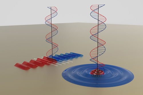 |
| Two different devices based on the herringbone pattern were presented in the Science paper: a rectangular array and a ring-shaped array (both interpreted in this illustration). Circularly polarized light with waves that wind in opposite directions gets split by both devices, with its waves routed in opposite directions. For a ring-shaped coupler, this means that plasmons are channeled either toward or away from the center of the structure. Intensity at the center of the ring can therefore be switched on and off by manipulating the polarization of the incoming light. (Image courtesy of Jiao Lin and Samuel Twist.)
|
|
"If you want to send a data signal around on a tiny chip with lots of components, then you need to be able to precisely control where it's going," says co-lead author Balthasar Müller, a graduate student at the Harvard School of Engineering and Applied Sciences (SEAS). "If you don't control it well, information will be lost. Directivity is such an important factor."
|
|
The coupler transforms incoming light into a wave called a surface plasmon polariton, a surface ripple in the sea of electrons that exists inside metals.
|
|
In the past, it has been possible to control the direction of these waves by changing the angle at which light strikes the surface of the coupler, but, as Müller puts it, "This was a major pain. Optical circuits are very difficult to align, so readjusting the angles for the sake of routing the signal was impractical."
|
|
With the new coupler, the light simply needs to come in perpendicularly, and the device does the rest. Acting like a traffic controller, it reads the polarization of the incoming light wave—which might be linear, left-hand circular, or right-hand circular—and routes it accordingly. The device can even split apart a light beam and send parts of it in different directions, allowing for information transmission on multiple channels.
|
|
The coupler consists of a thin sheet of gold, peppered with tiny perforations. But the precise pattern of these slits, arranged rather like herringbones, is where the genius lies.
|
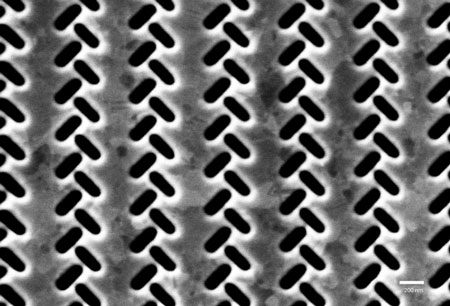 |
| An electron micrograph shows the nanoscale perforations at the surface of the plasmonic coupler. (Image courtesy of Jiao Lin and Balthasar Müller.)
|
|
"The go-to solution until now has been a series of parallel grooves known as a grating, which does the trick but loses a large portion of the signal in the process," says principal investigator Federico Capasso, Robert L. Wallace Professor of Applied Physics and Vinton Hayes Senior Research Fellow in Electrical Engineering at Harvard SEAS. "Now perhaps the go-to solution will be our structure. It makes it possible to control the direction of signals in a very simple and elegant way."
|
|
Because the new structure is so small—each repeating unit of the pattern is smaller than the wavelength of visible light—the researchers believe it should be easy to incorporate the design into novel technologies, such as flat optics.
|
|
Yet Capasso speaks most animatedly about the possibilities for incorporating the new coupler into future high-speed information networks that may combine nanoscale electronics (which currently exist) with optical and plasmonic elements on a single microchip.
|
|
"This has generated great excitement in the field," Capasso says.
|
|
Müller and Capasso were joined on this work by co-lead author Jiao Lin, a former SEAS postdoctoral fellow who is now at the Singapore Institute of Manufacturing Technology; and coauthors Qian Wang and Guanghui Yuan, of Nanyang Technological University, Singapore; Nicholas Antoniou, Principal FIB Engineer at the Harvard Center for Nanoscale Systems; and Xiao-Cong Yuan, a professor at the Institute of Modern Optics at Nankai University in China.
|

