| Oct 07, 2013 |
Particle accelerator on a chip
|
|
(Nanowerk News) Stanford engineers have helped create what may be the next big thing in particle accelerators – and it fits on a fingertip.
|
|
This “accelerator on a chip” was reported September 27th in the journal Nature ("Demonstration of electron acceleration in a laser-driven dielectric microstructure").
|
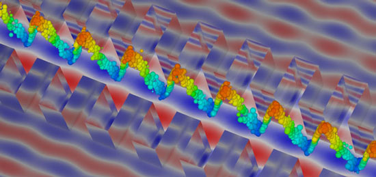 |
| A computer simulation of the glass accelerator chip shows the accelerating (orange) and decelerating (blue) components of the electromagnetic waves. The glass slits are the tooth-like features on both sides of the central electron conduit. (Ben Cowan/Tech-X Corp.)
|
|
The project included scientists from the U.S. Department of Energy’s (DOE) SLAC National Accelerator Laboratory, a linear accelerator two miles long.
|
|
Accelerators energize charged particles to accomplish a range of tasks from generating x-rays for medical imaging systems to unraveling the mysteries of matter.
|
|
They use electromagnetic waves to boost the energy of particles. Many conventional accelerators employ microwave radiation and bulky copper tubing to generate a wavy electric field. Particles surf these finely tuned waves, hitting swell after swell, and accelerating to higher and higher energies.
|
|
One of the ways the new device miniaturizes this process is by using a series of nanoscopic ravines etched into the chip by researchers at the Stanford Nanofabrication Facility (SNF). The SNF is a shared facility that provides researchers access to clean rooms and equipment to design, create, and characterize micro- and nano-scale devices.
|
|
On the accelerator chip, a laser shoots through the nanofabricated slits to create the waves that boost the particles’ energies. But unlike in large, conventional accelerators, the new device creates these waves in centimeters.
|
|
Synching the particles with the laser light is a challenge.
|
|
"Electrons are injected in bunches that are much longer than the accelerating phase of the laser field. So some electrons are actually decelerated," says Ken Leedle, an electrical engineering PhD student who helped implement the vacuum systems used in the experiments.
|
|
“But we’re already working with collaborators in Germany to address this,” says Leedle, who is with the research group of James S. Harris, the James and Ellenor Chesebrough Professor in the School of Engineering.
|
|
“In this first proof-of-principle demonstration, we were already able to see particle accelerating gradients that are much higher than what you can currently get with conventional accelerators,” says Edgar Peralta, a PhD candidate who was part of the nanofabrication team.
|
|
Peralta works in the lab of Robert L. Byer, professor of photon science and the William R. Kenan Jr., Professor of the School of Humanities and Sciences.
|

