| Mar 08, 2022 |
Growing wafer-scale 2D materials |
| (Nanowerk Spotlight) Two-dimensional van der Waals (vdW) materials are composed of strongly bonded layers of molecules with weak bonding between the layers. Layered van der Waals heterostructures are of great interest for electronic and photonic applications. |
| After graphene was first demonstrated in 2004, researchers have discovered thousands of other layered, atomically thin (two-dimensional, 2D) materials. Besides graphene, they include MXenes (atomic-thin transition metal carbides and nitrides), transition metal chalcogenides (TMDCs, including both metallic and semiconducting), 2D elemental semiconductors (black phosphorus (BP), tellurium (Te), 2D insulators (e.g., hexagonal boron nitride (h-BN and some oxides). |
| This huge variety of vdW layered 2D materials provides a large potential for advanced 2D nanoelectronics. However, for scalable applications, all vdW layered 2D materials face a common challenge: transitioning from micrometer-scale 2D flakes to wafer-scale. This is necessary for scaling up 2D vdW materials application in the high-end semiconductor industry. |
| Most vdW 2D materials are initially obtained through top-down synthesis methods, such as exfoliation, which can only prepare small flakes on a micrometer scale. Bottom-up growth can enable 2D flake growth over a large area. However, seamless merging of these flakes to form large-area continuous films with well-controlled layer thickness and lattice orientation is still a significant challenge. |
| The authors of a recent paper in Advanced Materials ("Growth of 2D Materials at the Wafer Scale") describe the structures, properties, wafer-scale growth methods, and applications of a number of representative vdW layered 2D materials. |
| For each material, they discuss in detail the status and recent developments of wafer-scale growth methods, including tube chemical vapor deposition (tube-CVD), metal-organic chemical vapor deposition (MOCVD), molecular beam epitaxy (MBE), atomic layer deposition (ALD), pulsed laser deposition (PLD), sputtering, solution process, and combination of these processes. |
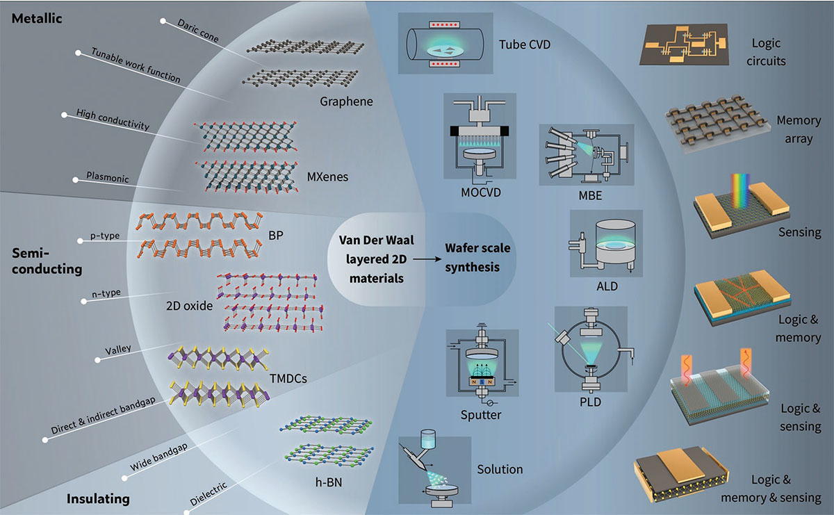 |
| Schematic showing various layered 2D materials, the methods used to grow them at the wafer-scale, and their integrated device applications. The shown 2D materials all have van der Waals (vdW) bonds in their lattices, and include: metallic or semimetallic, semiconducting, and insulating 2D materials. Wafer-scale growth methods include chemical and vacuum processes carried out using a wide range of temperatures. Various integrated devices that take advantage of 2D vdW films grown at wafer scale are also shown. (Reprinted with permission by Wiley-VCH Verlag) (click on image to enlarge) |
| The authors showcase various growth strategies for high-quality single-crystalline films at a wafer-scale, including growth of an isolated domain, growth of unidirectional domains, and conversion of oriented precursor. |
| They then discuss a number of examples for relevant devices and functional integrated applications that have been enabled by 2D material growth. |
| Developing high-quality single-crystalline 2D vdW films at the wafer scale is the precondition for having scalable 2D electronics and optoelectronics. Only by achieving 2D vdW layered films uniformly over an entire wafer is it possible for many 2D devices to be integrated onto a single chip. These devices include applications for photosensing, logic computing, memory, microscale ultracapacitors, and logic-in-memory. |
| The authors discuss several recent research works for using wafer-scale 2D vdW films in various integrated device applications. |
| As illustrated below, they show that 2D vdW layered materials are at different stages of development in terms of high-quality film growth at the wafer scale. Thus, future research directions in 2D materials growth will vary depending on the material in question. |
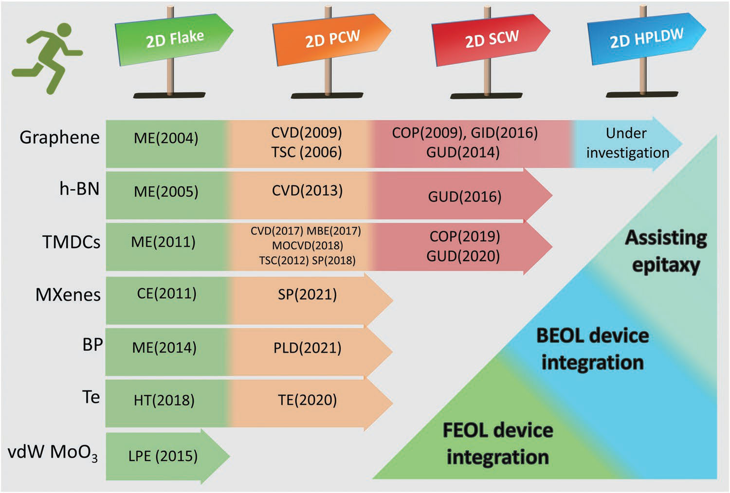 |
| Progress of growth processes for 2D vdW layered materials: from flakes to wafer scale. Abbreviations: PCW: polycrystalline wafer; SCW: single-crystalline wafer; HPLDW: high-purified and low-defect wafer; ME: mechanical exfoliation; CE: chemical etching; HT: hydrothermal reaction; LPE: liquid phase exfoliation; CVD: chemical vapor deposition; MOCVD: metal-organic chemical vapor deposition; MBE: molecular beam epitaxy; TSC: two-step conversion; SP: solution process; PLD: pulsed laser deposition; TE: thermal evaporation; GID: growth of an isolated domain; GUD: growth of unidirectional domains; COP: conversion of oriented precursors; BEOL: back-end-of-line; FEOL: front-end-of-line. (Reprinted with permission by Wiley-VCH Verlag) |
| The most progress has been made in graphene, where many research groups can now grow large-area single-crystalline graphene films. Efforts are currently focused on improving graphene quality by minimizing defects through clean growth methods. |
| The h-BN and TMDCs (especially MoS2) are at the stage of developing mono-oriented growth methods. Only several groups achieved their single-crystalline wafer-scale films, and many other TMDCs have not yet been achieved as high-quality films. |
| MXenes could be prepared as large-area films only through the solution process. High-quality large-area growth of MXenes by vacuum methods still needs to be explored, probably based on high-temperature vacuum deposition. |
| Elemental BP and Te p-type semiconductors have also reached the stage of large-area growth. Only one or two groups obtained their films over a large area. The Te film is grown by EBE and BP film by PLD. |
| The vdW MoO3 is still at the stage of basic physical property exploration. The discovery of its unique role in integrated circuits still needs time. |
| The goal that research into all these various vdW layered materials share is to develop growth methods of high-quality 2D films at a wafer scale. |
| The authors conclude by noting that current techniques must be optimized to improve film quality, new growth techniques need to be developed for single-crystal 2D wafers and for emerging 2D materials. All along the nature of the intended application should always be kept in mind as film properties vary depending on the target application. |
 By
Michael
Berger
– Michael is author of four books by the Royal Society of Chemistry:
Nano-Society: Pushing the Boundaries of Technology (2009),
Nanotechnology: The Future is Tiny (2016),
Nanoengineering: The Skills and Tools Making Technology Invisible (2019), and
Waste not! How Nanotechnologies Can Increase Efficiencies Throughout Society (2025)
Copyright ©
Nanowerk LLC
By
Michael
Berger
– Michael is author of four books by the Royal Society of Chemistry:
Nano-Society: Pushing the Boundaries of Technology (2009),
Nanotechnology: The Future is Tiny (2016),
Nanoengineering: The Skills and Tools Making Technology Invisible (2019), and
Waste not! How Nanotechnologies Can Increase Efficiencies Throughout Society (2025)
Copyright ©
Nanowerk LLC
|

Become a Spotlight guest author! Join our large and growing group of guest contributors. Have you just published a scientific paper or have other exciting developments to share with the nanotechnology community? Here is how to publish on nanowerk.com. |
