Nanotechnology News – Latest Headlines
California Energy Commission awards USD 1.6 million for energy storage research projects
The California Energy Commission has awarded $1,585,490 to spur research on projects including a battery system for grid-scale energy storage.
October 10, 2011 Read more
Shutting off inflammation with RNA-delivering nanoparticles
A new way to curb inflammatory cells could lead to treatments for diseases including atherosclerosis and cancer.
October 10, 2011 Read more
Graphene's 'Big Mac' creates next generation of chips
Researchers have for the first time demonstrated how graphene inside electronic circuits will probably look like in the future.
October 9, 2011 Read more
Global activist summit on nanotechnology calls on governments to protect people and environment
Some 30 activists representing 14 environmental, technology assessment and consumer organisations from Europe, the United States, Canada and Latin America met for the 4th International Nanotechnology Activist Summit in Berlin on October 6 and 7.
October 7, 2011 Read more
Are global honey bee declines caused by nanoparticles in diesel pollution?
Scientists are investigating a possible link between tiny particles of pollution found in diesel fumes and the global collapse of honey bee colonies.
October 7, 2011 Read more
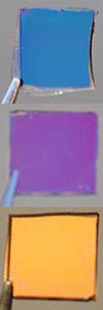
Colored solar cells could make display screens more efficient
A new kind of screen pixel doubles as a solar cell and could boost the energy efficiency of cell phones and e-readers. The technology could also potentially be used in larger displays to make energy-harvesting billboards or decorative solar panels.
October 7, 2011 Read more
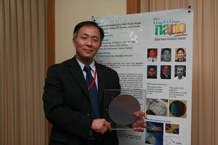
IBM's graphene nanoelectronics work wins ITRI's global nanotechnology innovation contest
IBM Research has emerged as the winner in the ITRI sponsored Global Nano Innovation Contest with its Graphene Nanoelectronics: Wafer Scale Single Atomic Layer Carbon RF Devices and Circuits.
October 7, 2011 Read more
Graphene shows unusual thermoelectric response to light
Finding could lead to new photodetectors or energy-harvesting devices.
October 7, 2011 Read more

Groundbreaking experimental research on reactive silicon compounds
Matthias Driess of TU Berlin receives Wacker Silicone Award 2011.
October 7, 2011 Read more
Doping for solar cells - New technique optimizes the generation of charge carriers
Researchers have been successful in substantially optimizing the electronic properties of organic semiconductors.
October 7, 2011 Read more
Verbraucheraspekte beim Umgang mit der Nanotechnologie
Der Ausschusses fuer Ernaehrung, Landwirtschaft und Verbraucherschutz des Deutschen Bundestages hielt am 24. Oktober eine Oeffentlichen Anhoerung zum Thema "Verbraucheraspekte beim Umgang mit der Nanotechnologie".
October 7, 2011 Read more
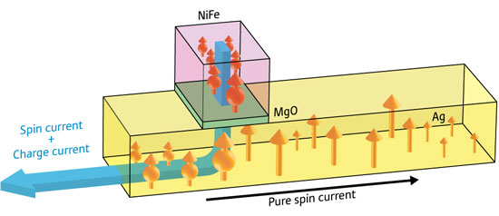
Moving forward, spin goes sideways
Improvements to specialized valves that separate spin and electron currents may lead to higher-density magnetic media.
October 7, 2011 Read more
Synthetic cells
Ion exchange leads to complex cell systems with inorganic membranes.
October 6, 2011 Read more
Hear live webcast tonight of top NJIT awardee detailing future of nanotechnology
Future of nanotechnology to detect viruses and more outlined.
October 6, 2011 Read more
Responsible development of nanotechnology
A new thesis by Ineke Malschat the Radboud University Nijmegen examines how ethically sound governance of nanotechnology may be possible in the current global world order.
October 6, 2011 Read more
Nanoinformatics 2011: Call for posters
Nanoinformatics 2011 will bring together informatics experts, nanotechnology researchers, and other stakeholders and potential contributors to advance Nanoinformatics 2020 Roadmap goals.
October 6, 2011 Read more
 Subscribe to our Nanotechnology News feed