Critical Dimension Scanning Electron Microscopy (CD-SEM): Precision Metrology for Nanoscale Fabrication
In the world of nanotechnology, where structures are measured in billionths of a meter, precise imaging and measurement techniques are essential. Critical Dimension Scanning Electron Microscopy (CD-SEM) is a powerful tool that enables researchers and manufacturers to visualize and quantify nanoscale features with incredible accuracy, playing a crucial role in the development and quality control of cutting-edge devices and materials.
What is Critical Dimension Scanning Electron Microscopy (CD-SEM)?
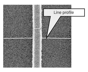
Critical Dimension Scanning Electron Microscopy (CD-SEM) is a specialized technique used for high-resolution imaging and precise measurement of nanoscale structures in semiconductor manufacturing and other nanotechnology applications. CD-SEM provides non-destructive, rapid, and accurate measurements of critical dimensions (CDs), such as linewidths, spacings, and hole diameters, with sub-nanometer resolution.
Principles of CD-SEM
CD-SEM operates on the principles of scanning electron microscopy, where a focused electron beam scans the surface of a sample, and the resulting secondary electrons are collected to form a high-resolution image. The key features of CD-SEM include:
- High Accelerating Voltage: CD-SEM systems typically operate at high accelerating voltages (1-5 kV) to achieve high resolution and minimize sample damage.
- Small Probe Size: The electron beam is focused to a small probe size (1-5 nm) to enable high-resolution imaging and precise measurement of nanoscale features.
- Low Landing Energy: The landing energy of the electron beam is carefully controlled to minimize sample charging and damage, ensuring accurate measurements.
- Advanced Electron Optics: CD-SEM systems employ advanced electron optics, such as aberration correctors and high-stability lenses, to achieve optimal resolution and measurement precision.
Applications of CD-SEM
CD-SEM finds extensive applications in the semiconductor industry and other nanotechnology fields:
Semiconductor Manufacturing
CD-SEM is an essential metrology tool in semiconductor manufacturing for process control and quality assurance. For example, in the production of advanced microprocessors, CD-SEM is used to measure the width of nanoscale transistor gates, ensuring they meet the design specifications for optimal performance and power efficiency. By monitoring these critical dimensions at various stages of the fabrication process, manufacturers can identify and correct any deviations, ultimately improving device yield and reliability.
Nanostructure Characterization
CD-SEM is widely used for the characterization of nanostructures, such as carbon nanotubes and semiconductor nanowires. In the development of novel nanomaterials for applications such as energy storage and conversion, CD-SEM enables researchers to accurately measure the diameter and length of individual nanostructures. These measurements provide valuable insights into the structure-property relationships of the materials, guiding the optimization of synthesis processes and device design.
Lithography Process Control
CD-SEM plays a crucial role in lithography process control, particularly in advanced patterning techniques such as extreme ultraviolet (EUV) lithography and directed self-assembly (DSA). In EUV lithography, which is used to create the intricate patterns of modern integrated circuits, CD-SEM measurements help optimize the exposure dose and focus settings to ensure the fidelity of the nanoscale features. By monitoring the critical dimensions and pattern uniformity across the wafer, lithography engineers can make real-time adjustments to maintain the desired pattern quality and minimize defects.
Challenges and Future Perspectives
As device dimensions continue to shrink and manufacturing processes become more complex, CD-SEM faces several challenges. One major challenge is the need for higher resolution and measurement precision to keep pace with the decreasing feature sizes. This requires the development of advanced electron optics, improved signal processing algorithms, and better sample preparation techniques.
Another challenge is the increasing demand for non-destructive and in-line metrology solutions. CD-SEM measurements are typically performed off-line and can be time-consuming, impacting throughput and productivity. Efforts are being made to develop in-line CD-SEM systems that can provide real-time measurements without interrupting the fabrication process.
Future developments in CD-SEM technology will focus on improving resolution, measurement speed, and automation. The integration of machine learning and artificial intelligence techniques will enable more intelligent and adaptive measurement strategies, enhancing the accuracy and efficiency of CD-SEM metrology. Additionally, the combination of CD-SEM with other complementary techniques, such as atomic force microscopy (AFM) and optical scatterometry, will provide a more comprehensive understanding of nanoscale structures and their properties.
Further Reading
ECS Transactions, Path to Better CD-SEM Condition Control for Advanced Technology Nodes
Handbook of Silicon Semiconductor Metrology, Critical Dimension Metrology and the Scanning Electron Microscope
Materials Science and Engineering: R: Reports, Nanoscale characterization of semiconductor materials and devices using scanning probe techniques
