Electrostatic Force Microscopy (EFM): Probing Nanoscale Electrical Properties
What is Electrostatic Force Microscopy?
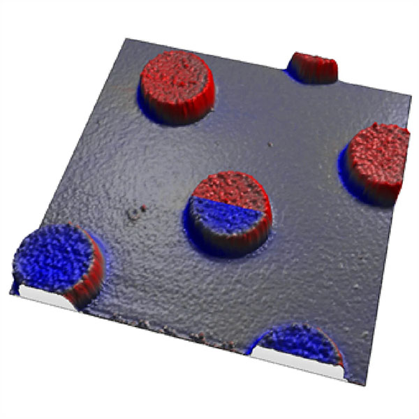
Electrostatic Force Microscopy (EFM) is a scanning probe microscopy technique that measures the electrostatic interactions between a conductive probe and a sample surface. EFM is a powerful tool for mapping the local electrical properties of materials at the nanoscale, providing valuable insights into their charge distribution, surface potential, and dielectric properties.
Principles of EFM
EFM is based on the principles of atomic force microscopy (AFM) but with an additional focus on electrostatic interactions. The key components and principles of EFM include:
- Conductive Probe: EFM uses a conductive probe, typically made of or coated with a metal like platinum or gold. The probe is mounted on a cantilever that oscillates near its resonance frequency.
- Voltage Application: A voltage is applied between the conductive probe and the sample surface. This voltage can be either DC or AC, depending on the specific measurement mode.
- Electrostatic Force Detection: The electrostatic force between the probe and sample depends on their respective voltages and the local electrical properties of the sample. This force causes a shift in the resonance frequency or amplitude of the cantilever oscillation, which is detected by the EFM system.
- Non-Contact Mode: EFM operates in a non-contact mode, where the probe does not make direct physical contact with the sample surface. This prevents damage to the sample and allows for non-invasive measurements.
EFM Measurement Modes
EFM can be operated in different measurement modes to extract specific electrical properties:
DC-EFM
In DC-EFM, a DC voltage is applied between the probe and sample. The electrostatic force depends on the surface potential difference between the probe and sample. By measuring the force as a function of the applied voltage, the local surface potential and work function can be determined.
AC-EFM
AC-EFM involves applying an AC voltage between the probe and sample. The resulting oscillating electrostatic force induces changes in the cantilever oscillation. By analyzing the amplitude and phase of the cantilever response, information about the local capacitance, dielectric constant, and charge distribution can be obtained.
Kelvin Probe Force Microscopy (KPFM)
KPFM is a variant of EFM that measures the contact potential difference (CPD) between the probe and sample. A feedback loop adjusts the DC voltage applied to the probe to nullify the electrostatic force. The nullifying voltage is equal to the CPD, providing a direct measure of the local work function.
Applications of EFM
EFM finds applications in various fields where understanding nanoscale electrical properties is crucial:
Semiconductor Characterization
EFM is widely used in the semiconductor industry to characterize the electrical properties of materials and devices. It can map the local doping concentration, detect charge traps, and investigate the performance of transistors and other electronic components.
Solar Cells and Photovoltaics
EFM is employed to study the charge transport and recombination processes in solar cells and photovoltaic materials. It can map the local potential distribution, identify charge accumulation sites, and assess the efficiency of charge extraction.
Energy Storage Materials
EFM is used to investigate the charge storage mechanisms in energy storage materials, such as batteries and supercapacitors. It can probe the local ionic distribution, detect charge inhomogeneities, and study the electrode-electrolyte interfaces.
Nanoelectronics and Spintronics
EFM is applied to characterize the electrical properties of nanoelectronic devices and materials, such as nanowires, carbon nanotubes, and graphene. It can also probe the spin-dependent transport in spintronic materials and devices.
Advantages and Limitations
EFM offers several advantages over other electrical characterization techniques:
- High spatial resolution, enabling nanoscale mapping of electrical properties
- Non-invasive and non-destructive measurements
- Ability to probe both surface and subsurface charge distributions
- Compatibility with various environmental conditions (vacuum, air, liquid)
However, EFM also has some limitations:
- Quantitative interpretation of EFM data can be challenging due to the complex nature of electrostatic interactions
- Requires conductive samples or the presence of a conductive layer on insulating samples
- Sensitivity to surface contamination and oxidation
- Potential influence of the probe on the local electrical properties
Future Perspectives
EFM continues to evolve with advancements in probe fabrication, instrumentation, and data analysis techniques. Future developments in EFM may include:
- Improved spatial and energy resolution through the use of novel probe designs and materials
- Integration with other scanning probe techniques for multidimensional characterization
- Development of advanced data processing algorithms for quantitative analysis and artifact reduction
- In-situ and operando EFM measurements to study dynamic electrical processes
As the demand for understanding nanoscale electrical properties grows, EFM will continue to play a vital role in the characterization and development of advanced materials and devices.
