| Posted: May 13, 2015 |
Nanotechnology improves methods for detecting polluting emissions |
| (Nanowerk News) Pollutants emitted by factories and car exhausts affect humans who breathe in these harmful gases and also aggravate climate change up in the atmosphere. Being able to detect such emissions is a critically needed measure. |
| New research by the Nanoparticles by Design Unit at the Okinawa Institute of Science and Technology Graduate University (OIST), in collaboration with the Materials Center Leoben Austria and the Austrian Centre for Electron Microscopy and Nanoanalysis has developed an efficient way to improve methods for detecting polluting emissions using a sensor at the nanoscale. The paper was published in Nanotechnology ("Single CuO nanowires decorated with size-selected Pd nanoparticles for CO sensing in humid atmosphere"). |
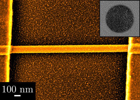 |
| Palladium nanoparticles were deposited on the entire wafer in an evenly distributed fashion, as seen in the background. They also attached on the surface of the copper oxide wire in the same evenly distributed manner, as seen in the foreground. On the upper right is a top view of a single palladium nanoparticle photographed with a transmission electron microscope(TEM) which can only produce black and white images. The nanoparticle is made up of columns consisting of palladium atoms stacked on top of each other. (Image: OIST) |
| The researchers used a copper oxide nanowire decorated with palladium nanoparticles to detect carbon monoxide, a common industrial pollutant. The sensor was tested in conditions similar to ambient air since future devices developed from this method will need to operate in these conditions. |
| Copper oxide is a semiconductor and scientists use nanowires fabricated from it to search for potential application in the microelectronics industry. But in gas sensing applications, copper oxide was much less widely investigated compared to other metal oxide materials. |
| A semiconductor can be made to experience dramatic changes in its electrical properties when a small amount of foreign atoms are made to attach to its surface at high temperatures. In this case, the copper oxide nanowire was made part of an electric circuit. The researchers detected carbon monoxide indirectly, by measuring the change in the resulting circuit’s electrical resistance in presence of the gas. They found that copper oxide nanowires decorated with palladium nanoparticles show a significantly greater increase in electrical resistance in the presence of carbon monoxide than the same type of nanowires without the nanoparticles. |
| The OIST Nanoparticles by Design Unit used a sophisticated technique that allowed them to first sift nanoparticles according to size, then deliver and deposit the palladium nanoparticles onto the surface of the nanowires in an evenly distributed manner. This even dispersion of size selected nanoparticles and the resulting nanoparticles-nanowire interactions are crucial to get an enhanced electrical response. The OIST nanoparticle deposition system can be tailored to deposit multiple types of nanoparticles at the same time, segregated on distinct areas of the wafer where the nanowire sits. In other words, this system can be engineered to be able to detect multiple kinds of gases. The next step is to detect different gases at the same time by using multiple sensor devices, with each device utilizing a different type of nanoparticle. |
| Compared to other options being explored in gas sensing which are bulky and difficult to miniaturize, nanowire gas sensors will be cheaper and potentially easier to mass produce. |
| The main energy cost in operating this kind of a sensor will be the high temperatures necessary to facilitate the chemical reactions for ensuring certain electrical response. In this study 350 degree centigrade was used. However, different nanowire-nanoparticle material configurations are currently being investigated in order to lower the operating temperature of this system. |
| "I think nanoparticle-decorated nanowires have a huge potential for practical applications as it is possible to incorporate this type of technology into industrial devices,” said Stephan Steinhauer, a Japan Society for the Promotion of Science (JSPS) postdoctoral research fellow working under the supervision of Prof. Mukhles Sowwan at the OIST Nanoparticles by Design Unit. |
| Source: By Joykrit Mitra, Okinawa Institute of Science and Technology Graduate University |

