| Jun 05, 2019 |
Photoelectric detection of individual nitrogen-vacancy centers in diamond(Nanowerk News) NIMS, the University of Tsukuba, the German University of Ulm and others have jointly succeeded in obtaining the spin state readout of electrons in diamond crystals using an electrical technique called photoelectric detection. |
| Unlike conventional methods, this technique enabled detection of individual spin states at room temperature in a simple manner and is therefore potentially applicable to the development of quantum sensing devices, such as magnetic sensors with nanoscale spatial resolution ("Photoelectrical imaging and coherent spin-state readout of single nitrogen-vacancy centers in diamond"). |
 |
| Single nitrogen-vacancy diamond. (Image: NIMS) |
| Serious efforts have been made to develop quantum sensors capable of sensitively responding to electric fields, magnetic fields and temperatures within materials and biological systems. Nitrogen-vacancy (NV) centers—crystalline defects consisting of a nitrogen atom (N) and an adjacent lattice vacancy (V) that occur infrequently in the diamond lattice—are capable of confining electron spins within a nanoscale space and remaining in the same quantum state for prolonged periods of time. |
| Because of these desirable properties, NV center defects may be useful in the development of highly sensitive quantum sensors with nanoscale special resolution. The spin state readouts of NV centers are currently obtained by irradiating NV centers with laser light and detecting the fluorescent light they emit. |
| However, the sensitivity of this method had been limited by its ability to detect only one photon out of dozens. |
| This joint research team succeeded for the first time in photoelectrically detecting individual NV centers with high imaging contrast. In this particular research project, photoelectric detection refers to a technique used to detect electric current generated by an NV center after its irradiation with laser light. One of our most significant achievements was mapping individual NV centers using this technique. |
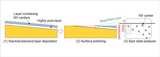
| Diamond samples conducive to this technique were prepared using the following unique process. First, we deposited a highly pure diamond layer and a diamond layer containing a trace amount of nitrogen (i.e., a NV center-containing diamond layer) on the slanted surface of a diamond substrate consecutively. We then polished the surface of the deposited diamond in a specific manner to expose cross-sections of the individual layers. |
| Certain areas of the polished diamond sample had NV centers distributed only in proximity to the upper surface above the at least 10 µm thick highly pure diamond layer in which NV centers are absent. We mapped individual NV centers in these areas by means of photoelectric detection. These results indicated that the technique we have developed may be applicable to the development of quantum sensing technologies. |
| The technique developed in this research, which enables detection of the spin states of NV centers in diamond by simply applying a small electrode to its surface, may serve as a key instrument in the miniaturization of quantum sensing devices and quantum information processing devices. |
| Source: University of Tsukuba |
|
Subscribe to a free copy of one of our daily Nanowerk Newsletter Email Digests with a compilation of all of the day's news. |

