| Aug 13, 2020 |
Engineers manipulate color on the nanoscale, making it disappear(Nanowerk News) Most of the time, a material’s color stems from its chemical properties. Different atoms and molecules absorb different wavelengths of light; the remaining wavelengths are the “intrinsic colors” that we perceive when they are reflected back to our eyes. |
| So-called “structural color” works differently; it’s a property of physics, not chemistry. Microscopic patterns on some surfaces reflect light in such a way that different wavelengths collide and interfere with one another. For example, a peacock’s feathers are made of transparent protein fibers that have no intrinsic color themselves, yet we see shifting, iridescent blue, green, and purple hues because of the nanoscale structures on their surfaces. |
| As we become more adept at manipulating structure at the smallest scales, however, these two types of color can combine in even more surprising ways. Penn Engineers have now developed a system of nanoscale semiconductor strips that uses structural color interactions to eliminate the strips’ intrinsic color entirely. |
| The researchers experimented with nanoscale strips of a two-dimensional semiconductor, tungsten disulfide, arranged on a gold backing. |
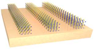 |
| The researchers experimented with nanoscale strips of a two-dimensional semiconductor, tungsten disulfide, arranged on a gold backing. (Image: University of Pennsylvania) |
| Though the strips should absorb orange light and thus appear a shade of blue, they appear to have no color at all. |
| Fine-tuning such a system has implications for holographic displays and optical sensors. It could also pave the way for new types of microlasers and detectors, fundamental elements of long-sought-after photonic computers. |
| The study was led by Deep Jariwala, assistant professor in the Department of Electrical and Systems Engineering, along with lab members Huiqin Zhang, a graduate student, and Bhaskar Abhiraman, an undergraduate. |
| It was published in Nature Communications ("Hybrid exciton-plasmon-polaritons in van der Waals semiconductor gratings"). |
| The researcher’s experimental system consists of nanoscale strips of a two-dimensional semiconductor, tungsten disulfide, arranged on a gold backing. These strips, only a few dozen atoms thick, are spaced out at sub-optical wavelength sizes, allowing them to give off the type of structural color seen in butterfly wings and peacock feathers. |
| “We played with the dimensions of this system, took a lot of experimental measurements, and ran a lot of simulations. Then we noticed something weird,” Abhiraman says. “If the dimensions of these strips were just right, the absorption of orange light, which should be intrinsic to the material, disappeared! In other words, the coating that comprised of these stripes is insensitive to incoming light and only shows the properties of the underlying substrate.” |
| “Other nanophotonics researchers have previously shown before that structural color and these intrinsic absorptions can interact; this is called ‘strong coupling.’ However, no one has seen this kind of disappearance before, especially in a material that is otherwise supposed to absorb nearly 100 percent of the light,” Jariwala says. “In the example of bird feathers or butterfly wings, it’s the biological material’s nanoscale structures which gives them iridescent colors, since those materials don’t have much intrinsic color on their own. But if a material does have a strong intrinsic color, we show that one can do the opposite and make it disappear with appropriate nanostructuring. In some ways, it is cloaking the material’s intrinsic color from its response to light.” |
| Investigating this phenomenon involves understanding how intrinsic color works on a subatomic level. An atom’s electrons are arranged in different concentric levels, depending on how many electrons that element has. Depending on the available spaces in those arrangements, an electron can jump to a higher level when it absorbs the energy from a certain wavelength of light. The wavelengths that are capable of exciting electrons in this way determine which are absorbed and which are reflected, and thus a material’s intrinsic color. |
| Nanophotonics researchers like Jariwala, Zhang and Abhiraman study even more complicated interactions between electrons and their neighbors. When atoms are arranged in repeating crystalline patterns, such as those found in the two-dimensional strips of tungsten disulfide, their electron layers overlap into contiguous bands. These bands are what allow conductive materials to pass charges from electron to electron. Semiconductors, like tungsten disulfide, are ubiquitous in electronics because the interplay between their electron bands give rise to useful phenomena that can be manipulated with external forces. |
| In this case, the interaction of light and electrical charge within the semiconductor strips produced the unprecedented “cloaking” effect. |
| “When the electron is excited by orange wavelengths, it creates a vacancy known as a hole, leaving the crystal with a tightly bound pair of opposite charges called an exciton,” Jariwala says. “Because light is a form of electromagnetic radiation, its electromagnetic field can interact with this charge excitation and in special circumstances cancel it out, so that an observer would see the orange of the gold substrate instead of the blue of the strips on top of it.” |
| In their paper, Jariwala and his colleagues showed that the structural color effects and the intrinsic exciton absorption interaction can be modeled with the exact same mathematics as coupled oscillators: masses bouncing on springs. |
| “We applied this model and discovered that under certain conditions, this disappearance effect can be reproduced,” Zhang says. “It’s beautiful that a trick from classical mechanics can explain the way our structure interacts with light.” |
| This type of structural color, or the lack of it, can be used to make nanometer thickness coatings that are engineered to be insensitive to incoming light, meaning the coating appears to be the same color as material underneath it. Different spatial arrangements of those nanoscale features could produce the opposite effect, allowing for brilliant holograms and displays. Traditionally, manipulating such features has been difficult, as the required materials were much thicker and harder to fabricate. |
| “Since this structural color that we observe is also very sensitive to its surrounding environment,” Abhiraman says, “one can imagine make cheap and sensitive colorimetric sensors for chemicals or biological molecules if paired with the right chemical bait.” |
|
|
| “Another area of potential application is integrated spectrometers and photodetectors on a chip,” he says. “Even here, traditional semiconductor materials such as silicon have been hard to use since their optical properties are not conducive for strong-absorption. By virtue of the 2D materials’ quantum confined nature, they absorb or interact with light very strongly, and their sheet-like structure makes it easy to place or deposit or coat them on arbitrary surfaces.” |
| The researchers think that the most powerful application of their system might be in photonic computers, where photons replace electrons as the medium for digital information, massively improving their speed. |
| “Hybridization of light and matter has long been used in optical communication switches and has been envisioned as the operating principle for the ultra-low threshold power lasers necessary for photonic computing,” Jariwala says. “However, it has been difficult to get such devices to work at room temperatures in a reliable and desired manner. Our work shows a new path towards making and integrating such lasers on arbitrary substrates, especially if we can find and replace our current 2D semiconductors with ones that like to emit a lot of light.” |
| Source: University of Pennsylvania |
|
Subscribe to a free copy of one of our daily Nanowerk Newsletter Email Digests with a compilation of all of the day's news. |

