| Jun 01, 2021 |
Metamaterial improves sensitivity of infrared absorption spectroscopy 100 times
(Nanowerk News) A research team, comprised of members of the Korea Institute of Machinery & Materials (KIMM) under the Ministry of Science and ICT and UNIST, developed a metamaterial absorber that significantly enhances the detection of harmful substances or biomolecules, and published their results in Small Methods ("Ultrasensitive Molecule Detection Based on Infrared Metamaterial Absorber with Vertical Nanogap").
|
|
The joint research team led by Principal Researcher Dr. Joo-Yun Jung of the Nano-Convergence Mechanical Systems Research Division at KIMM and Professor Jongwon Lee of UNIST developed a metamaterial that enhances infrared absorption spectroscopy through 100-fold amplification of detection signals. The proposed metamaterial is a special functional material with vertical nanogaps of a smaller size than infrared wavelength.
|
|
Infrared spectroscopy is a technique that identifies components based on patterns of reflected light by measuring the properties of molecules to absorb infrared of their intrinsic frequencies. If only small traces of the target substance are detected, the results will not be as significant due to the small difference in light intensity.
|
|
The proposed metamaterial gathers and releases light energy at once, thereby inducing a larger intensity of light that can be absorbed by molecules. The amplified signals allow more distinct results to be obtained even when working with small traces of substances.
|
|
Cross-shaped nanoantennas were formed in a metal-insulator-metal configuration. The middle insulating layer had a thickness of 10 nm; vertical gaps were employed to maximize light absorption by molecules.
|
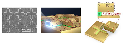 |
| Left) SEM image of the metamaterial absorber developed by KIMM and UNIST. Top view shows cross-shaped antenna. Center) Side view of the microstructure of the metamaterial absorber developed by KIMM and UNIST. Right) Structure of the metamaterial absorber developed by KIMM and UNIST. Figure shows 10 nm vertical nanogaps. Right) Structure of the metamaterial absorber developed by KIMM and UNIST. Figure shows 10 nm vertical nanogaps. (Image: KIMM) (click on image to enlarge)
|
|
Inyong Hwang, a researcher of the Department of Electrical Engineering at UNIST, said, "The proposed metamaterial achieved a record-high difference of 36% in our demonstration on a monolayer with a thickness of 2.8 nm. This is the best record achieved to date among monolayer detection experiments."
|
|
The proposed metamaterial can be easily mass-produced and offers low-cost manufacturing. While high-resolution beam lithography was required to form microstructures on metamaterial surfaces, the team's SEIRA platform relies on more affordable nanoimprint lithography and dry-etching processes.
|
|
Dr. Joo-Yun Jung, principal researcher of KIMM, said, "Using the nanoimprint process, we can obtain metamaterials in the metal-insulator-metal configuration, and process them into desired patterns. On top of that, the dry etching process allows mass production of microstructured metamaterials."
|
|
Professor Jongwon Lee of UNIST said, "Our study is the first to induce near-field enhancement and resolve near-field exposure using vertical gaps. The technique is expected to have vast applications, especially for infrared sensors used in the detection of biomolecules, harmful substances, and gases."
|


