| Jan 03, 2022 |
3D semiconductor particles offer 2D properties
(Nanowerk News) When it comes to creating next-generation electronics, two-dimensional semiconductors have a big edge. They’re faster, more powerful and more efficient. They’re also incredibly difficult to fabricate.
|
|
Three-dimensional semiconductor particles have an edge, too – many of them – given their geometrically varied surfaces. Cornell researchers have discovered that the junctures at these facet edges have 2D properties, which can be leveraged for photoelectrochemical processes – in which light is used to drive chemical reactions – that can boost solar energy conversion technologies.
|
|
This research, led by Peng Chen, the Peter J.W. Debye Professor of Chemistry in the College of Arts and Sciences, could also benefit renewable energy technologies that reduce carbon dioxide, convert nitrogen into ammonia, and produce hydrogen peroxide.
|
|
The group’s paper published in Nature Materials ("Inter-facet junction effects on particulate photoelectrodes"). The paper’s lead author is postdoctoral researcher Xianwen Mao.
|
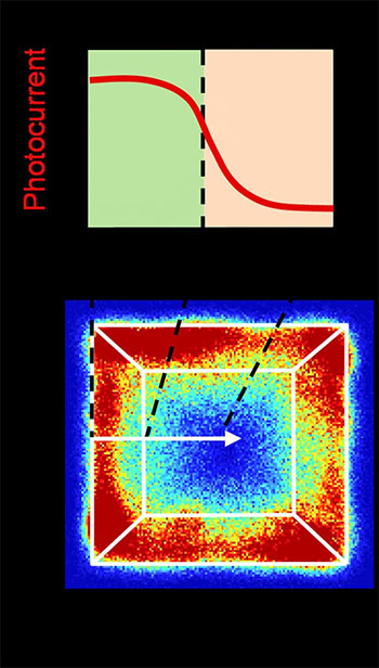 |
| A high-resolution map of a photocatalyst particle shows the transition zones of reactivity and the corresponding spatial variation of photoelectrochemical performance across the inter-facet edge. (Image: Cornell University)
|
|
For their study, the researchers focused on the semiconductor bismuth vanadate, particles of which can absorb light and then use that energy to oxidize water molecules – a clean way of generating hydrogen as well as oxygen.
|
|
The semiconductor particles themselves are anisotropically-shaped; that is, they have 3D surfaces, full of facets angled toward each other and meeting at edges on the particle surface. However, not all facets are equal. They can have different structures that, in turn, result in different energy levels and electronic properties.
|
|
“Because they have different energy levels when they join at an edge, there’s a mismatch, and the mismatch gives you a transition,” Chen said. “If you had a pure metal, it wouldn’t have this property.”
|
|
Using a pair of high-spatial-resolution imaging techniques, Mao and Chen measured the photoelectrochemical current and surface reactions at multiple points across each facet and the adjoining edge in between, and then used painstaking quantitative data analysis to map the transition changes.
|
|
The researchers were surprised to find that the three-dimensional particles can actually possess the electronic properties of two-dimensional materials, in which the transition happens gradually across the so-called transition zone near the edge where the facets converge – a finding that had never been envisioned and could not have been revealed without high-resolution imaging.
|
|
Mao and Chen hypothesize the width of the transition zone is comparable to the size of the facet. That would potentially give researchers a way to “tune” the electronic properties and customize the particles for photocatalytic processes. They could also tune the properties by changing the widths of the near-edge transition zones via chemical doping.
|
|
“The electronic property is dependent on which two facets are converging at an edge. Now, you basically can design materials to have two desired facets merge. So there’s a design principle,” Chen said. “You can engineer the particle for better performance, and you can also dope the material with some impurity atoms, which changes the electronic property of each facet. And that will also change the transition associated with this inter-facet junction. This really points to additional opportunities for three-dimensional semiconductor particles.”
|

