| Jun 26, 2023 |
Using electric fields to control the movement of defects in crystals
(Nanowerk News) An international team of researchers, led by Professor Yu Zou (MSE), is using electric fields to control the motion of material defects. This work has important implications for improving the properties and manufacturing processes of typically brittle ionic and covalent crystals, including semiconductors — a crystalline material that is a central component of electronic chips used for computers and other modern devices.
|
|
In a study published in Nature Materials ("Harnessing dislocation motion using an electric field"), researchers from U of T Engineering, Dalhousie University, Iowa State University and Peking University, present real-time observations of dislocation motion in a single-crystalline zinc sulfide that was controlled using an external electric field.
|
|
“This research opens the possibility of regulating dislocation-related properties, such as mechanical, electrical, thermal and phase-transition properties, through using an electric field, rather than conventional methods” says Mingqiang Li (MSE PhD candidate), the first author of the new paper.
|
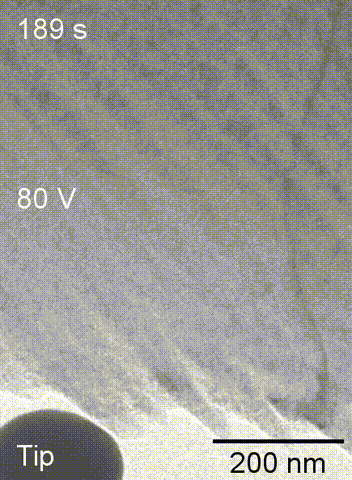 |
| A real-time observation of an individual dislocation moving under an electric field using transmission electron microscopy. The dislocation moves back and forth depending on the magnitude and direction of the electric field. (Video: Zou Research Group in MSE)
|
|
In materials science, dislocation is a linear crystallographic defect within a crystal structure that contains an abrupt change in the arrangement of atoms.
|
|
It is the most important defect in crystalline materials, says Zou, since it can affect the strength, ductility, toughness, thermal and electrical conductivities of crystalline materials, such as steel used in airplanes and silicon used in chips.
|
|
In crystalline solids, good ductility and formability are generally achieved by dislocation movement. As such, metals that have highly mobile dislocations can be deformed into final products through compression, tension, rolling and forging — for example, aluminum cans are punched out to form the shape.
|
|
In contrast, ionic and covalent crystals generally suffer from poor dislocation mobility that make them too brittle to process using mechanical methods, and as a result, unsuited to a broad range of manufacturing techniques. In the case of semiconductors, they are typically too brittle to be rolled and forged.
|
|
“The primary driving force of dislocation motion has been commonly limited to mechanical stress, restricting the processing routes and engineering applications of many brittle crystalline materials,” says Zou.
|
|
“Our study provides direct evidence of dislocation dynamics controlled by a non-mechanical stimulus, which has been an open question since the 1960s. We also rule out other effects on the dislocation motion, including Joule heating, electron wind force and electron beam irradiation.”
|
|
The study used an in-situ transmission electron microscopy to observe dislocation motion in zinc sulfide, which was driven solely by an applied electric field in the absence of mechanical loading. Dislocations that carried negative or positive charges were both triggered by the electric field.
|
|
The researchers observed dislocations moving back and forth while changing the direction of the electric field. They also found that the mobilities of dislocations in an electric field also depends on their dislocation types.
|
|
Since most semiconductors are brittle due to their poor dislocation mobility, the electric-field-controlled dislocation motion in this new study may be used to enhance their mechanical reliability and formability, says Li.
|
|
“In addition, our work offers an alternative method to reduce defect density in semiconductors, insulators and aged devices that doesn’t require traditional tedious thermal annealing, which uses temperature over time to reduce defects of a material,” he adds.
|
|
While this initial study has been focused on zinc sulfide, the team is planning to explore a wide range of materials, from covalent crystals to ionic crystals.
|
|
“As we work towards the application of this technology, our aim is to collaborate with the materials and manufacturing industries, particularly semiconductor companies, to develop a new manufacturing process to reduce defect density and improve the properties and performance of semiconductors,” says Zou.
|

