| Oct 04, 2023 |
Integrating 2D materials for on-chip photonics
(Nanowerk News) Recently, the introduction of nonlinear optical functions in integrated optics has sparked significant enthusiasm. Demonstrations have shown the potential for integrated photonic platforms. Furthermore, large-scale manufacturing capability and affordability have motivated developing fully integrated, nonlinear optical devices for various applications like on-chip spectroscopy, on-chip quantum computations and communications, efficient multiplexing for data communications, on-chip metrology, bio-sensing, or LIDARs.
|
|
In a new paper published in Light: Advanced Manufacturing ("Hybrid integration of 2D materials for on-chip nonlinear photonics"), Professors Vincent Pelgrin and Zhipei Sun and their team reviewed the range of hybrid photonic integration structures.
|
Key Takeaways
|
|
Integration of nonlinear optical functions is opening new avenues in photonic platforms.
Large-scale manufacturing and affordability are propelling the development of integrated nonlinear optical devices.
Recent publication delves into the assortment of hybrid photonic integration structures, spotlighting innovative approaches in silicon photonics.
Challenges like Two Photon Absorption (TPA) in Silicon are identified, with alternative materials like stoichiometric SiN being explored.
Hybrid integration of two-dimensional (2D) materials like graphene is highlighted as a promising approach to enhance nonlinear performance of waveguides.
|
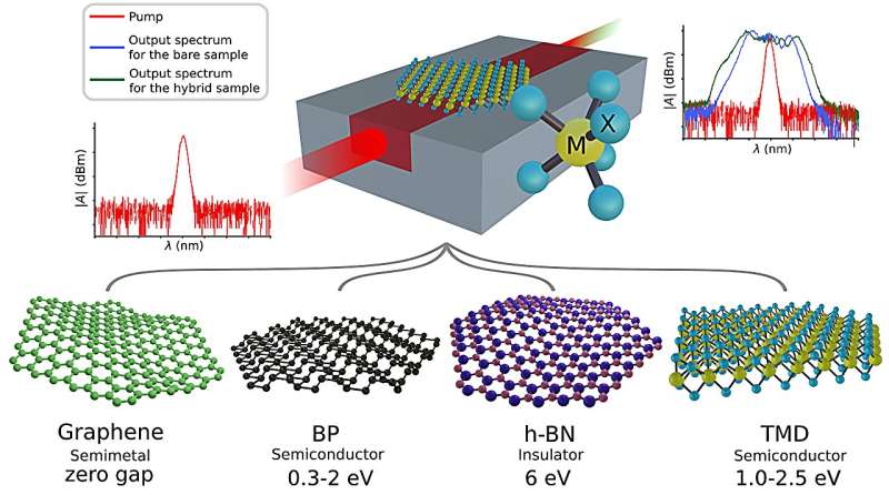 |
| Conceptual representation of the hybrid integration of 2D materials. Below are lists of the most common 2D materials with their bandgaps that have been integrated with waveguide structures. The inset spectra show the input (red) spectrum, and the output broadened spectra (blue for intrinsic waveguides and green for the 2D material integrated waveguides) during a typical pulse broadening experiment. (Image: Vincent Pelgrin, Yoon Hoon Hahn, Eric Cassan, and Zhipei Sun)
|
|
Integrating these active functions in silicon photonics has attracted much attention too. The possible compatibility with CMOS processes and the overall low cost of the platform make it very attractive to industry, with devices directly suitable for dense optical circuit fabrication.
|
|
These deep integration capabilities make the Si-compatible platform an interesting testbed for the transposition. However, silicon photonics presents some impediments when exploiting nonlinear optical processes. These primarily include the weak nonlinear responses of the most common materials compatible with its clean room processes or the presence of free carriers.
|
|
Although Si demonstrates high nonlinearity in the C-band range, it suffers from Two Photons Absorption (TPA) due to its low bandgap. Unfortunately, most classical materials compatible with silicon integration lack strength in optical nonlinearities. The stochiometric SiN nonlinear refractive index is nearly two orders of magnitude lower than Si.
|
|
Impressive demonstrations using various silicon-based materials have generated integrated optical functions. These include supercontinuum sources, frequency combs, and photon pair sources through spontaneous four-wave mixing. In some fields, communities have pushed for more efficient devices exhibiting high performance with low power consumption.
|
|
Researchers have demonstrated annealed SiN waveguides with loss levels of a few dB/m, but the required pump power remained high. Achieving sufficient nonlinear processes necessitated long waveguides, thus making optical functions demanding for fully integrated devices.
|
|
Alternatively, materials like Si-rich waveguides or engineering carrier density using p-i-n junctions have shown promising results. However, drawbacks exist. Si-rich waveguides still exhibit TPA. Meanwhile, employing multiple p-i-n junctions adds complexity to devices and circuits. Hence, the need for solutions to this limitation remains strong.
|
|
Another approach introduces highly nonlinear materials to the on-chip platform, harnessing the effective properties of these materials. This approach boosts their nonlinear performance through integration strategy. Over the past decade, researchers have tested several materials. Chalcogenides are a popular alternative to Si-based materials.
|
|
In the quest to identify disrupting nonlinear optical materials, two-dimensional (2D) layered materials have emerged as extremely promising. These materials possess third-order susceptibility up to two orders of magnitude higher than Si. While graphene is the most widely known material in this category, other 2D materials like Transition Metal Dichalcogenides (TMDs) where M is a metal atom and X is a chalcogen are also gaining attention. BP is also receiving increasing attention.
|
|
The principle behind hybrid integration is incorporating high-performance 2D materials into existing integration platforms, thus increasing the overall effective nonlinear performance of the waveguides. However, hybrid integration presents challenges as 2D materials are still not fully understood. Carefully handling the impact of their addition to integrated structures is necessary.
|
|
The review presents recent progress in the field and the perspectives of Pelgrin, Sun and their team. They briefly introduced the theoretical background of hybrid integration of 2D materials for different integrated optics platforms. The aim is describing key steps from modeling and design to characterization. This will hopefully serve as a guideline for future works in related fields, thus solving one of the obstacles encountered with integrated nonlinear photonics.
|

