| Jun 18, 2026 |
3D-printed glowing ceramics could shrink future photonic devices
Laser 3D printing turns YAG:Ce ceramics into precise, light-emitting microstructures for compact sensors, LEDs, optical circuits and radiation detectors.
(Nanowerk News) Modern technologies, from smartphones and LED lighting to medical sensors and space equipment, rely heavily on materials that can both emit and control light. One of the most widely used materials for this purpose are ceramics, specifically yttrium aluminum garnet (YAG) doped with cerium (Ce³⁺). This combination produces a bright yellow light and is commonly used in white LEDs and laser-based lighting systems.
|
|
However, while these materials are well established in bulk form (such as powders or coatings), it has remained very difficult to shape them into tiny, complex three-dimensional (3D) structures with high precision.
|
|
This research was motivated by the growing demand for miniaturized photonic devices—precise systems that manipulate light for optical communication, sensing, and advanced imaging applications. To meet this demand, scientists need ways to form light-emitting materials directly into microscopic 3D shapes, while maintaining their optical performance and stability.
|
|
Traditional manufacturing methods cannot readily achieve high resolution, 3D architectures, or the required crystalline purity, limiting their applicability.
|
|
To address this challenge, the researchers developed a new fabrication approach that combines chemical synthesis and advanced laser-based 3D nano-printing. First, a liquid precursor material is prepared via a sol–gel process, in which metal-containing compounds are mixed to form a light-sensitive resin. This resin is then shaped using multiphoton laser lithography. A tightly focused laser polymerizes the desired 3D structure inside the material, solidifying only the regions where the light is most intense, allowing extremely fine features to be created.
|
|
The study was published online in the journal of Opto-Electronic Advances ("Luminescent YAG:Ce3+ 3D micro-structures via multi-photon laser lithography").
|
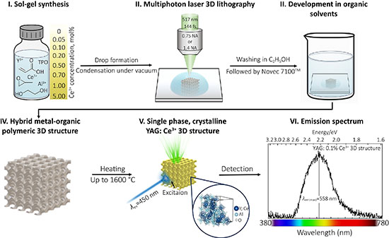 |
| A photoresin was prepared with varying Ce3+ concentrations (0–5 mol%), and then it was structured via MP3DL, followed by development and pyrolysis, to yield crystalline, single-phase, luminescent YAG:Ce3+ 3D microstructures. The resulting microstructures exhibit a characteristic Ce3+ emission band peaking at 558 nm under 450 nm excitation, confirming the successful formation of a single-phase cubic YAG:Ce3+ and its luminescent functionality. (Image: Reproduced from DOI:10.29026/oea.2026.250338, CC BY)
|
|
After printing, the structures are carefully heated in several stages. This heat treatment removes organic components and transforms the material into a dense, crystalline ceramic in its original shape, even as it shrinks. The final result is a single-phase, robust, and highly precise 3D object that emits light efficiently.
|
|
This work demonstrates a reliable method to create microscopic light-emitting ceramic structures, opening new possibilities for compact photonic devices and advanced optical systems.
|
|
The Laser Nanophotonics group led by Prof. Mangirdas Malinauskas, in collaboration with the Materials Science group (Greta Merkininkaitė), both groups from Vilnius University, Lithuania, and Arturo Susarrey Arce group from the University of Twente, Netherlands, has developed a method for producing miniature light-emitting ceramic structures with high precision.
|
|
This work addresses a major challenge in modern photonics: the fabrication of complex 3D microscopic components that are both thermally stable and optically functional. By integrating chemical synthesis, high-resolution laser-based 3D printing, and controlled high-temperature processing, the researchers demonstrate a method for creating materials capable of efficient light emission at very small scales.
|
|
This technology is particularly well-suited for applications in next-generation photonic and optoelectronic devices. These include micro-scale light sources for advanced displays, compact sensors for environmental or biomedical monitoring, integrated optical circuits that guide and manipulate light, and electronic circuits that control electrical signals.
|
|
It could also play a role in laser-based lighting systems, micro-scintillators for radiation detection, and even miniaturized components for space technologies, where materials must withstand extreme conditions.
|
|
In terms of societal impact, the ability to precisely fabricate 3D light-emitting materials, specifically single-phase crystalline YAG:Ce³⁺ rather than amorphous or multiphase materials reported in earlier studies, could lead to more energy-efficient and reliable devices. The use of single-phase crystalline materials ensures more stable and efficient light emission, which is critical for high-performance applications.
|
|
For example, improved LED and laser technologies could reduce energy consumption in lighting and displays, while compact sensors could enhance healthcare diagnostics or environmental monitoring. Additionally, integrating such high-quality materials directly into microdevices could simplify the manufacturing process and reduce costs over time.
|
|
Looking ahead, the next steps for this research are to achieve greater precision, explore additional luminescent materials, and integrate multiple optical functionalities into a single structure. Researchers may also focus on scaling up production and adapting the method for industrial use.
|
|
Overall, these findings represent a significant step toward the future of “3D-printed micro-photonics,” where light-emitting and light-controlling components are directly fabricated at the microscale. This could transform how optical devices are designed and manufactured, paving the way for smarter, more compact, and more efficient technologies across many fields.
|

