| Jun 18, 2026 |
Real-time microscopy reveals how semiconductor nanowires grow, and how bismuth seeds can speed their formation
Scientists captured tellurium nanowire growth in liquid in real time, showing seed formation, material competition and bismuth-assisted deposition.
(Nanowerk News) Scientists from the National Graphene Institute at The University of Manchester and Sun Yat-sen University, have captured the growth of semiconducting tellurium nanostructures in liquid in real time, revealing how tiny seed particles form, grow into nanowires and compete for material as the structures develop.
|
|
The study, published in Matter ("In situ liquid-phase TEM electrodeposition of tellurium nanostructures"), also shows that adding bismuth seed particles can make tellurium easier to deposit under specific electrodeposition conditions used in the experiments.
|
 |
| Artistic render illustrating the electrodeposition growth of tellurium nanowires from solution. (Image: The University of Manchester)
|
|
The work focuses on tellurium, a semiconductor of interest for electronic, thermoelectric and optoelectronic applications, where performance depends strongly on the size and shape of the nanostructures produced. Although liquid-phase synthesis is a scalable and relatively low-cost way to make these materials, it has been difficult to observe exactly how anisotropic tellurium structures begin to form and evolve during growth.
|
|
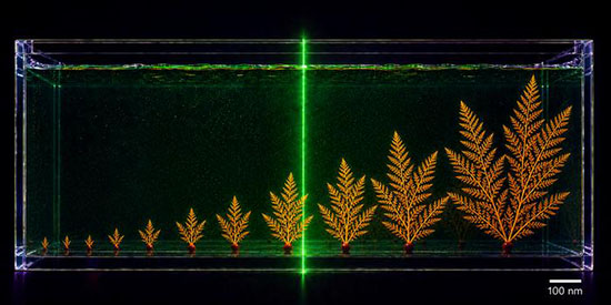
Using liquid-phase transmission electron microscopy, the researchers tracked the early stages of tellurium formation at the nanoscale. They found that tellurium first appears as spherical seed particles, which then give rise to multiple nanowires. During growth, nearby wires compete for available material, affecting local growth speed and branching.
|
|
Across the experiments, local nanowire growth rates were measured in the range of 1 to 15 nm per second, depending on electron flux and the presence of neighbouring structures.
|
|
Professor Sarah Haigh, corresponding author at The University of Manchester and the National Graphene Institute, said: “This study lets us see, in real time, how tellurium nanowires emerge and evolve in liquid. By directly observing nucleation, growth and branching at the nanoscale, we can begin to understand how to control these processes much more precisely. That matters because the performance of tellurium-based materials depends strongly on their size and shape.”
|
|
A second key finding was that bismuth seed nanoparticles dramatically change how tellurium grows. In the microscopy experiments, bismuth increased the number of nucleation sites and promoted more highly branched, fern-like structures. Follow-up electrodeposition experiments confirmed that bismuth also lowers the reducing potential needed for tellurium deposition and can substantially increase the amount of tellurium deposited under the same conditions.
|
|
Together, these results show how insights from real-time microscopy can guide more effective materials synthesis outside the microscope.
|
|
Dr Yi-Chao Zou, co-corresponding author, said: “One of the most exciting aspects of this work is that the behaviour we observed in the liquid cell translated into conventional electrodeposition experiments. We found that bismuth seeding not only promotes tellurium nucleation but also makes deposition easier and more productive at a fixed potential. That opens up new possibilities for designing tellurium nanostructures with tailored morphologies for future device applications.”
|
|
The study, a collaboration between Sun Yat-sen University, The University of Manchester, the National Graphene Institute and Beijing Institute of Technology, suggests that real-time microscopy can do more than describe nanostructure growth. In this case, it identified a specific way to alter nucleation behaviour and improve deposition under defined experimental conditions.
|
|
That could help researchers refine how tellurium nanostructures are produced for device-relevant studies, while keeping claims closely tied to the systems tested here. The team report the findings could help accelerate the optimisation of low-dimensional nanostructures for electronics, energy conversion and sensing applications.
|

