| Mar 18, 2022 |
Are 2D interfaces really completely flat?
(Nanowerk News) When two or more atomically thin sheets of materials – like graphene – are placed on top of each other, their properties change and a material with novel hybrid properties emerges.
|
|
The in-plane stability of the individual 2D materials is provided by strong covalent bonds. The stacked materials are called van der Waals heterostructures because the atomically thin layers are not mixed through a chemical reaction but rather attached to each other via a weak so called van der Waals interaction – similar to how a sticky tape attaches to a flat surface.
|
|
The atomically thin sheets are not necessarily uniform. They can be subject to mechanical deformation that result in defects, such as bubbles and wrinkles that occur during exfoliation and transfer.
|
|
The lack of perfect flatness of individual layers forming a van der Waals heterostructure has implications for interface properties, such as those formed by metal contacts or insulating layers.
|
|
Although numerous researchers have investigated defects of standalone 2D materials, there are not many studies on the overall morphology and flatness of 2D interfaces, especially their flatness under different conditions.
|
|
Hoping to develop a deeper understanding of 2D interfaces and interface engineering, in a new paper in ACS Nano ("Are 2D Interfaces Really Flat?"), researchers reveal the intricacy of various 2D interfaces at the length scale of an array of electronic devices (12.5 µm in total) and under the impact of stacking and metalization. In this work, they characterize and compare the flatness of the hexagonal boron nitride (hBN)-2D and metal-2D interfaces down to angstrom resolution.
|
|
For their study of 2D interfaces the researchers set up two device arrays (as shown in the figure below). In device array A, the 2D-2D interface (the interfaces between two different 2D-layered materials) is the hBN-MoS2 in the channel region. In a typical 2D transistor, the 3D-2D interfaces (the interfaces between 3D materials and 2D materials) include the 3D metal-2D contact interface and 3D dielectric-2D interface. These 3D-2D interfaces can be found in both device array A and B.
|
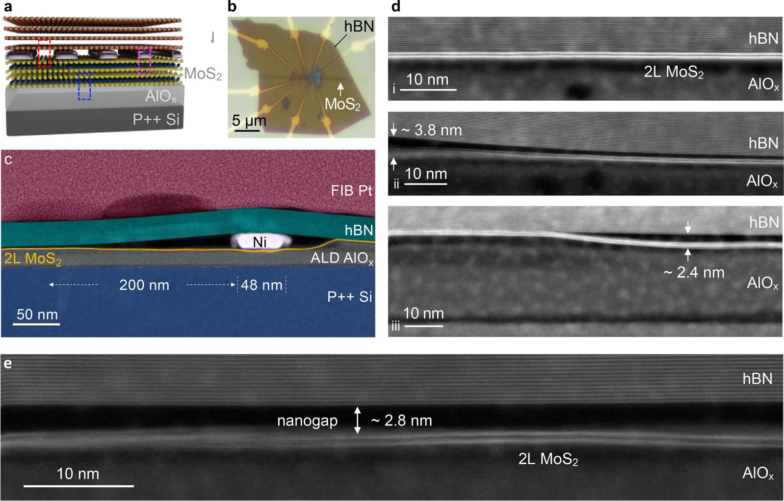 |
| Schematics and high-angle annular dark-field scanning transmission electron microscopy (HAADF-STEM) images of the hBN-MoS2-AlOx interface in Device array A. (a) Cross-sectional schematic of the device. The red, blue, and magenta dashed boxes represent hBN-MoS2, MoS2-AlOx, and Ni-MoS2 interfaces, respectively. (b) Optical image of the devices with hBN encapsulation. (c) False-colored STEM image of a contact region. The thickness of the Ni contact is ∼16 nm. (d) The hBN-MoS2 and MoS2-AlOx interfaces in the channel region with (i−iii) representing different locations. In (i), the interfaces are flat and intimate, whereas in (ii−iii), the hBN and MoS2 diverge to form nanogaps. (e) An example nanogap of ∼2.8 nm formed between hBN and 2L MoS2 in the channel region. (Reprinted with permission by American Chemical Society)
|
|
Correlating the interface deformation with the corresponding device performance, the authors discovered how the nonplanar interfaces can affect the device characteristics.
|
|
Their observations have broad implications in applications such as electronic devices and nanofluidics where 2D materials are transferred onto patterned contacts and for devices where metal contacts are deposited onto 2D materials.
|
|
For instance, the team reports that the hBN stacking process clearly has a mechanically aggressive effect on the flatness of the interfaces and films. And relevant for MoS2-based field-effect transistors: the metal deposited from the commonly used e-beam evaporator can also distort the Ni-MoS2 interface, especially near the contact edge where there is more pressure due to the arc shape of the contacts.
|
|
Concluding their report, the authors note that the delicate nature of 2D interfaces should be considered when characterizing their properties. S show promise for contact engineering and device performance optimization. Furthermore, the effects of strain and interface engineering will be especially pronounced for devices that involve transferring and stacking 2D materials onto predeposited metal contacts or gates.
|
 By
Michael
Berger
– Michael is author of four books by the Royal Society of Chemistry:
Nano-Society: Pushing the Boundaries of Technology (2009),
Nanotechnology: The Future is Tiny (2016),
Nanoengineering: The Skills and Tools Making Technology Invisible (2019), and
Waste not! How Nanotechnologies Can Increase Efficiencies Throughout Society (2025)
Copyright ©
Nanowerk LLC
By
Michael
Berger
– Michael is author of four books by the Royal Society of Chemistry:
Nano-Society: Pushing the Boundaries of Technology (2009),
Nanotechnology: The Future is Tiny (2016),
Nanoengineering: The Skills and Tools Making Technology Invisible (2019), and
Waste not! How Nanotechnologies Can Increase Efficiencies Throughout Society (2025)
Copyright ©
Nanowerk LLC