| Posted: August 5, 2009 |
New super lattice structure offers effective means for developing quantum functional devices |
|
(Nanowerk News) Shinichi Shikata (Deputy Director of Diamond Research Center and concurrently Leader), Hideyuki Watanabe (Research Scientist) and others of the Device R&D Team, the Diamond Research Center of the National Institute of Advanced Industrial Science and Technology (AIST) have succeeded in the vapor-phase synthesis of a stack of nanometer-scale thin films of diamond using carbon isotopes 12C and 13C, which differ in mass. Electrons and holes were confined to a single material for the first time using the diamond stack.
|
|
Among all available materials, diamond has the optimal characteristics with respect to hardness, thermal conductivity, light transmission wavelength range, and chemical stability. Furthermore, as a semiconducting material, diamond shows excellent characteristics in terms of breakdown electric field and carrier mobility, suggesting prospective application to electrochemical and semiconductor devices, in addition to mechanical and optical applications. As a semiconductor, diamond appears to have a promising future in high-performance materials for power devices and quantum computers. Studies are still underway because the aspects of diamond as a semiconducting material have not yet been fully explored.
|
|
In this study, diamonds were synthesized using a microwave plasma-assisted chemical vapour deposition (CVD) method, from methane (CH4) gases containing only 12C or 13C carbon isotopes. A super lattice structured diamond was prepared by alternately depositing 25 diamond layers, each containing only 12C or 13C, with thickness of 30 nm. The layered diamond was irradiated with an electron beam and the electron-hole recombination was measured. It was found that recombination occurred only in the 12C-containing diamond layers, indicating that electrons and holes were confined to 12C layers. So far, the confinement of electrons and holes has been reported only with a combination of different materials (GaAs/AlGaAs, InGaAs/InP, etc.); this study reports the first success with a single material. The result makes structural design of a single material using the semiconductor band-gap engineering possible, and it offers an effective means for developing ultrafast devices and quantum functional devices.
|
|
The result of the study appears in the electronic version of the American journal Science on June 12, 2009.
|
|
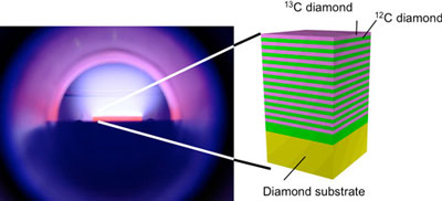
| A view into the microwave plasma-assisted CVD reactor and a schematic illustration of the structure after deposition of diamond film.
|
|
Social Background for Research
|
|
Diamond is an insulating material normally, but it is also a semiconducting material, in which the resistivity is controlled to 16 orders of magnitude by adding impurities. One of excellent properties of diamond is that the thermal conductivity is 6 times as large as those of the widely adopted heat sink materials including copper. The prospective electronic applications using diamond include power devices that are needed for the power control of electric appliances, lying at the center of energy-saving technologies. The saving of electrical power energy through upgraded power devices is one of the prioritized energy-related innovative technologies in the 'Cool Earth – Innovative Energy Technology Program' of the Ministry of Economy, Trade and Industry for drastic reduction of CO2. Furthermore, diamond is now a prospective material for quantum bits in future quantum computers.
|
|
Today, this feasibility has become even more promising: room temperature operation is made feasible; the lifetime of quantum bits is improving; and quantum entanglement, needed for enabling quantum calculation, is substantiated.
|
|
History of Research
|
|
Aiming at developing new applied technologies, the Diamond Research Center of AIST conducts studies on diamond integrating semiconducting properties of diamond with its hardness, thermal conductivity, elastic modulus, optical transmittance, chemical stability, and electrochemical properties, those are the most outstanding characteristics among all materials. In the past, the center developed a technology for fabricating a large-sized diamond single crystal. Including the present study, the center has also studied various devices and their basic material aspects, aiming at the development of diamond power devices.
|
|
Details of Research
|
|
In this study, diamond was synthesized by microwave plasma-assisted CVD. Source gases were methane (CH4) and hydrogen (H2); when methane was made with only the 12C isotope, the deposited diamond layer contained only 12C, and when methane was made with only the 13C isotope, only 13C is contained in the deposited layer. A super lattice structure was fabricated by alternately stacking 25 diamond layers, each with thickness of 30 nm. Figure 1 shows the schematic illustration of a super lattice structure and the results of chemical composition analysis in the vertical direction using secondary ion mass spectrometry (SIMS) for the 13C/12C diamond layer stack. The results very clearly show that 12C and 13C diamond layers are stacked. This is the first study reporting the fabrication of a nanometer-sized super lattice structure with diamond.
|
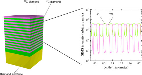 |
| Fig. 1 Super lattice structure of isotopically enriched diamond films grown in this work and compositional depth profiles measured by SIMS.
|
|
Irradiating an electron beam on the stacked thin-film structure to generate electrons and holes, their recombination processes was measured. It was found that recombination occurred only in the diamond layers with 12C, suggesting that electrons and holes were confined there. As Fig. 2 shows, in the super lattice structure, only light due to recombination of electrons and holes in the layers with 12C. For comparison, measurements were made on the samples with only a single nanometer-sized layer, and recombination was detected both in the 12C and the 13C layers. The energy difference (difference in band gaps) of 20 mV between the two diamond layers, as shown in Fig. 3, indicates that electrons and holes move away from the 13C diamond layers into the 12C layers and electrons and holes are confined.
|
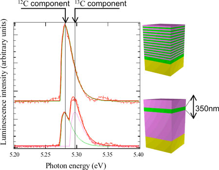 |
| Fig. 2 Electron-hole recombination luminescence by electron beam irradiation
|
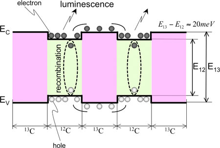 |
| Fig. 3 Simplified schematic diagram of electron and hole confinement (Ec and Ev are conduction band-edge and valence band-edge, respectively.)
|
|
So far, the confinement of electrons and holes has been realized only with a super lattice structure using heterogeneous junctions of different materials (GaAs/AlGaAs, InGaAs/InP, etc.), which differ in energy, while the lattice constants are similar. High electron mobility transistors and semiconductor lasers are the semiconductor devices designed and fabricated by using this important phenomenon. The new type of confinement using homojunctions(same material), which was previously considered impossible and has been achieved in this study, is attributable to the relatively large energy difference between the isotopes of diamond. The homojunction is made of the same crystal and offers the merit that the electrons and holes do not recombine at the junction interface, and so various device structures will be fabricated easily.
|
|
The confinement of electrons and holes using isotopic homojunctions is an important finding. Using only diamond, it is now possible to control the energy state of electrons and holes and their distribution, which intrinsically depend on the material, by using the semiconductor band-gap engineering. Thus, we now have an effective means for realizing ultrafast devices and quantum functional devices. This finding may revolutionize the field of diamond applications.
|
|
Future Schedule
|
|
For practical device applications of diamond, even higher material quality is needed, and our challenges include the reduction of defects, epitaxial film growth on large-sized wafers, and control of electrons and holes. Furthermore, regarding the confinement of electrons and holes using isotopes, the lifetime of electrons and holes inside the isotopes, recombination at the homojunction interface, and mobility of electrons and holes must be evaluated in detail, and the data will be examined whether they can effectively be used to design quantum functional devices. The technology shall be developed horizontally, such as for creating 13C quantum bits. We shall establish basic technologies through future studies on new electronic applications for diamond.
|

