| Dec 05, 2011 |
Partnership for progress in electronics at Berkeley Lab strengthened by new lab-industry investment
|
|
(Nanowerk News) As manufacturers pack more and more circuitry into the tiny microchips on which electronic technologies depend, ultraviolet light's narrow wavelengths are essential for creating the densely patterned chips of the future. Leading semiconductor and emerging-technology firms have recently renewed their long collaboration with the U.S. Department of Energy's Lawrence Berkeley National Laboratory (Berkeley Lab) to build facilities and instruments for advanced extreme-ultraviolet lithography (EUVL), including microlithography test tools too costly for individual manufacturers.
|
|
Since the early 2000s, Berkeley Lab's Center for X-Ray Optics (CXRO) has worked with semiconductor companies to develop the infrastructure needed for world-leading research and development in the field of EUVL, contributing basic research and development essential to the health of the U.S. industry as a whole before individual firms enter competition.
|
|
In total funding valued at almost $10 million, Berkeley Lab has recently reinvested $1.5 million in royalties from other licensed technologies to build a new clean room and wafer processing facility at Beamline 12 of the Lab's Advanced Light Source (ALS), where CXRO researchers will create the MET5 microfield exposure tool. To build the tool, industry will provide several million dollars plus valuable optics, with additional support to operate the new facility.
|
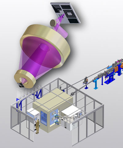 |
| The MET5 microlithography tool at the Advanced Light Source's beamline 12.0.1 will be housed in an enclosure inside a new clean room with wafer-processing facilities immediately adjacent, built by Berkeley Lab. The MET5 tool, funded by industry, incorporates a state-of-the-art, 8-nanometer optic.
|
|
Horst Simon, Berkeley Lab's Deputy Director and one of the world's leading experts in computer technology, demonstrated Berkeley Lab's commitment to maintaining the currency of the Advanced Light Source's services to its valued users by arranging for investment of Lab funds in the new facilities. "This is an excellent example of how the Department of Energy is engaging in innovative collaborations with industry, and how our national labs contribute to maintaining, and indeed increasing, U.S. leadership in a field that has been largely created in this country. We must maintain this type of continued technology investment in order to remain competitive as a nation in today's global economy."
|
|
Says Roger Falcone, director of the Advanced Light Source, "The Lab's investment encouraged industry to continue our fruitful research partnership, assuring them that their investment here will be leveraged to enable the leading-edge research needed in the coming decades."
|
|
"The MET5 will be a unique instrument with double the effective resolution of the best tools now in commercial use," says CXRO's director, Patrick Naulleau, a staff scientist in the Lab's Materials Sciences Division. "MET5 and the new wafer-processing facility at ALS Beamline 12 will allow us to develop and test photosensitive materials capable of transferring patterns on the nanoscale, the future domain of semiconductor lithography technology."
|
|
Extreme ultraviolet lithography embraces a range of technologies, including special mirrors and photomasks that reflect soft-x-ray light, to image circuit patterns onto the surface of semiconductor wafers. Since the wavelength of extreme ultraviolet light is much shorter than visible light, EUVL can produce chips whose circuitry has much smaller features, enabling orders-of-magnitude more memory capacity and operating speed than today's best electronic devices.
|
|
The MET5 microlithography tool uses the extraordinarily bright beams of EUV light produced by the Advanced Light Source to project circuit features, measured in billionths of a meter, onto semiconductor wafers. The exposed patterns on the wafers are a few nanometers in dimension, and will be instantly processed under clean room conditions for evaluating the results. In future commercial facilities, larger designs will be stacked one on another at high speeds to produce working circuitry; the test facility is a necessary first step to try out new approaches.
|
|
"To insure that tomorrow's technology will be successful," Naulleau says, "we have to develop every aspect of the process in advance."
|

