| Dec 16, 2011 |
Imec launches Center for Advanced Metrology Solutions |
| (Nanowerk News) Imec has officially launched the Center for Advanced Metrology Solutions (CAMS). This center draws on the extensive expertise of imec to commercially offer a high quality service for scanning spreading resistance microscopy and a range of products and solutions to enable and support electrical atomic force microscopy measurements. |
| Scanning spreading resistance microscopy (SSRM) - a technique invented at imec - is an electrical atomic force microscopy (AFM) - based technique which provides high-resolution quantitative carrier distributions in 1D, 2D & 3D semiconductor structures, such as thin films, solar cells, MOSFETs, FinFETs, TFETs, etc. Recent developments in resolution and the extension to other semiconducting materials (SiGe, Ge, InGaAs, InP, ...) has led to a strong, growing interest from the semiconductor community for the characterization of advanced structures. To enable the entire community to benefit from these developments, imec now offers a commercial SSRM service to external customers through its newly created Center for Advanced Metrology Solutions. |
| A key role in the success of high resolution SSRM is played by the full diamond AFM probes that have been developed at imec. These probes enable sub-nm resolution SSRM measurements and are more durable than conventional diamond-coated tips for high-force contact AFM measurements. With the creation of CAMS these unique probes become commercially available. |
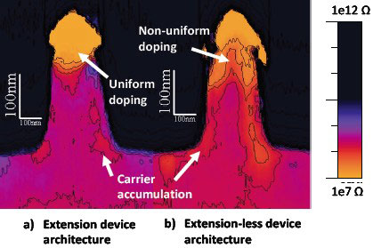 |
| SSRM image of a FinFET structure obtained with full diamond tips. (© J. Mody et al., IEDM 2011, Washington, US) |
| Furthermore, CAMS will offer dedicated calibration standards and resolution qualification structures. The calibration standards are made of a stack of uniformly doped Si layers (with thicknesses varying from 0.2 to 5 microns) and are ideally suited for quantification measurements, for spreading resistance profiling or AFM-based techniques (SSRM, SCM, KPFM, SMM, ...). The resolution qualification standards consist of a thin uniform layer of SiO2 confined between highly doped grown poly-Si and implanted Si. These oxide layers (with thicknesses varying between 0.3 and 10nm) are excellent for evaluating the resolution of electrical probes or imaging techniques such as scanning electron microscopy. |
| By offering extensive tailor-made training, customers can also profit from the extensive know-how available at imec. Interested SSRM users can be trained in every aspect of these electrical measurements, from sample preparation and electrical measurements to data interpretation and quantification. Moreover, the imec CAMS may also serve as a research partner for applying AFM-based metrology to new devices and materials and implementing novel characterization concepts. |
| For more information on the imec Center for Advanced Metrology Solutions, see www.imec.be/cams or contact imec at [email protected]. |
| Source: imec |

