| Jan 19, 2012 |
Nanoscale bouncing gold droplets |
| (Nanowerk News) When a pebble is dropped onto the surface of a pond, a droplet of water bounces up from the surface. The same thing happens when a focussed laser-beam strikes the surface of a thin metal film – the metal can be locally melted by the laser light and it can bounce up from the metal surface as a metallic droplet. |
| Now Dr Paul Warburton and Edward Osley of the London Centre for Nanotechnology and UCL's Department of Electrical Engineering have collaborated with colleagues from Belgium, Russia, Germany, Singapore and Bulgaria to show that this phenomenon can be used to make nanoscale metallic droplets (see paper in Advanced Materials: "Plasmon-Enhanced Sub-Wavelength Laser Ablation: Plasmonic Nanojets"). |
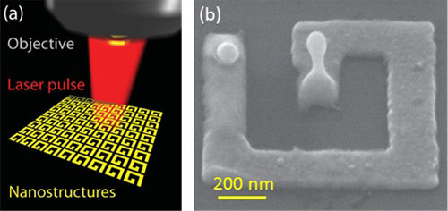 |
| (a) Schematic of the experiment; (b) Electron micrograph of a single gold "G". A gold nano-droplet has been melted by the laser pulse but then re-solidifies in mid-bounce. |
| In the experiment, infra-red laser light with wavelength 800 nm is focussed onto a gold film which has been patterned into a series of tiny "G"-shapes (see figure a). The width of the lines which make up each "G"-shape is 200 nm. When the laser hits the "G", it causes an electronic current to flow in the gold. This current heats up the gold, which can lead to local melting of the gold and the formation of the bouncing gold droplet (see figure b). What's interesting about this experiment is that the radius of the gold droplet is only 40 nm or so – i.e. 20 times smaller than the wavelength of the laser light which caused the melting to happen. This comes from the clever design of the geometry of the "G" which focusses the electric field of the infra-red light as it hits the metal surface. Furthermore by changing the polarisation of the laser light it's possible to controllably shift the part of the "G" which gets melted. |
| The work has a number of possible applications, including the manufacture of gold nanoparticles for medical applications such as cancerous tumour detection. In the electronics sector this method may be suitable for nanofabrication of interconnects in next-generation integrated circuits. |
| Source: London Centre for Nanotechnology |

