| Posted: May 12, 2008 |
3D carbon nanotube components integrated on carbon nanotube wafer |
|
(Nanowerk News) National Institute of Advanced Industrial Science and Technology (AIST) manufactured integrated 3D carbon-nanotube components by using single-layer carbon nanotubes. A "carbon-nanotube wafer" developed by densely aligning carbon nanotubes enabled to use microfabrication techniques of lithography.
|
|
The new technology made it possible to form any shape of electronic parts in any place. For example, AIST integrated more than a thousand 3D carbon-nanotube electronic parts on a substrate and electrically drove the component.
|
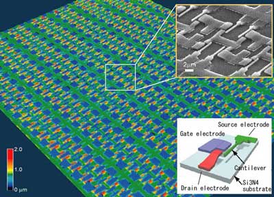 |
| Laser and electron microscope images of a 3D electronic component with integrated carbon nanotubes
|
|
The carbon-nanotube wafer is manufactured as follows: (1) A Si substrate is linearly patterned with a catalyst. (2) Carbon-nanotube films are made and vertically aligned on the Si substrate by using the "water adding CVD method" (Super Growth Method), which AIST developed in 2004. (3) By immersing the substrate in a liquid and pulling it out, carbon-nanotube films are laid down on the substrate. (4) As the liquid dries, those carbon-nanotube films become denser and attached firmly to the substrate to form a carbon-nanotube wafer.
|
|
The carbon-nanotube film in (2) has a density of 0.03g/cc with vertically-aligned carbon nanotubes whose diameter is 2.8nm on average. The carbon-nanotube wafer made in (4), after becoming denser, is shaped like a bar with the density of 0.5g/cc.
|
|
The carbon-nanotube wafer has machine characteristics of being light and robust. At the same time, it is very pliable, and its wires do not break even when bent to more than 90°. As for the electric property, its electric resistivity is 0.008Ω·cm in the direction parallel to the alignment of the carbon nanotubes and 0.20Ω·cm in the direction vertical to the alignment, showing an anisotropy.
|
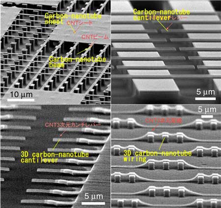 |
| Electron microscope images of various carbon-nanotube structures. (Clockwise from upper left) carbon-nanotube beams and sheets on Si pillars, carbon-nanotube cantilevers, 3D wiring, and 3D cantilevers.
|
|
The carbon-nanotube wafer does not break even when a resist for photomask is applied. Therefore, it can be formed into any shape by techniques of lithography. It is also possible to form carbon-nanotube structures, such as cantilever shapes, in the chases prepared on the Si substrate.
|
|
Furthermore, the carbon-nanotube wafer itself can retain a 3D shape. In fact, AIST fabricated a 3D cantilever and 3D wiring with integrated carbon nanotubes.
|
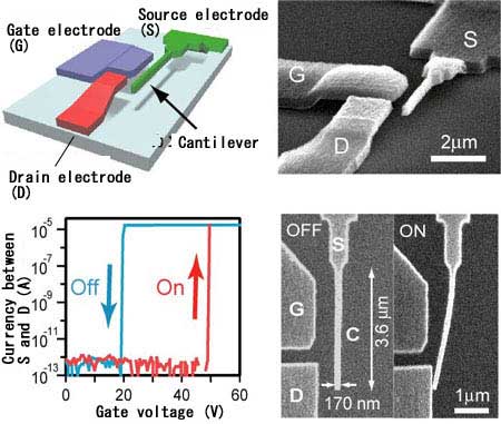 |
| A carbon-nanotube relay (upper left), its electric property (lower left) and electron microscope images (right).
|
|
It can be electrically driven because its carbon-nanotube structure provides a conductive property. For example, the institute fabricated and drove a carbon-nanotube relay whose electrodes are all composed of carbon nanotubes. It succeeded in mechanical switching of the carbon-nanotube cantilever by applying a voltage to gate electrodes (Fig 5).
|
|
AIST plans to evaluate the physical properties of the carbon-nanotube wafer and develop a carbon-nanotube component that takes advantage of the properties. Also, it puts emphasis on cooperation with companies and universities.
|
|
The study results announced this time was published in the online version of Nature Nanotechnology, a science magazine in the UK May 4, 2008.
|

