3D printing on the micro- and nanometer scale (w/video)
(Nanowerk News) At the Photonics West, the leading international fair for photonics taking place in San Francisco (USA) this week, Nanoscribe GmbH, a spin-off of Karlsruhe Institute of Technology (KIT), presents the world’s fastest 3D printer of micro- and nanostructures. With this printer, smallest three-dimensional objects, often smaller than the diameter of a human hair, can be manufactured with minimum time consumption and maximum resolution. The printer is based on a novel laser lithography method.
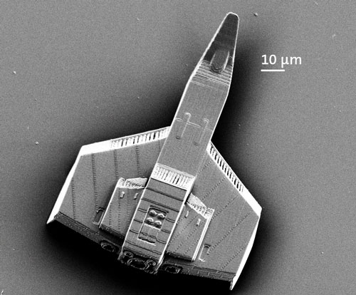
Printing on the micrometer scale: Writing time for a miniaturized spacecraft is reduced to less than one minute without loss of quality. (Photo: Nanoscribe)
“The success of Nanoscribe is an example of KIT’s excellent entrepreneurial culture and confirms our strategy of specifically supporting spin-offs. In this way, research results are transferred rapidly and sustainably to the market,” says Dr. Peter Fritz, KIT Vice President for Research and Innovation. In early 2008, Nanoscribe was founded as the first spin-off of KIT and has since established itself as the world’s market and technology leader in the area of 3D laser lithography.
Last year, 18 spin-offs were established at KIT. The 3D laser litho-graphy systems developed by Nanoscribe – the spin-off can still be found on KIT’s Campus North - are used for research by KIT and scientists worldwide. Work in the area of photonics concentrates on replacing conventional electronics by optical circuits of higher performance. For this purpose, Nanoscribe systems are used to print polymer waveguides reaching data transfer rates of more than 5 terabits per second.
Biosciences produce tailored scaffolds for cell growth studies among others. In materials research, functional materials of enhanced performance are developed for lightweight construction to reduce the consumption of resources. Among the customers are universities and research institutions as well as industrial companies.
This video shows a realtime recording of the 3D micro printing process by two-photon polymerization. It starts with the CAD model of a Hellcat spaceship from Wing Commander Saga and uses a 3D printer Photonic Professional GT to print a polymer model on the microscale. The final structure is then inspected with a scanning electron microscope (SEM). Overall printing time was less than 50 seconds for the ship with dimensions 125µm x 81µm x 26.8µm (l x w x h). The length of the spaceship is approximately equal to the diameter of a human hair.
Increased Speed: Hours Turn into Minutes
By means of the new laser lithography method, printing speed is increased by factor of about 100. This increase in speed results from the use of a galvo mirror system, a technology that is also applied in laser show devices or scanning units of CD and DVD drives. Reflecting a laser beam off the rotating galvo mirrors facilitates rapid and precise laser focus positioning. “We are revolutionizing 3D printing on the micrometer scale. Precision and speed are achieved by the industrially established galvo technology. Our product benefits from more than one decade of experience in photonics, the key technology of the 21st century,” says Martin Hermatschweiler, the managing director of Nanoscribe GmbH.
Mechanism: Two-photon Polymerization
The direct laser writing technique underlying the 3D printing method is based on two-photon polymerization. Just as paper ignites when exposed to sunlight focused through a magnifying glass, ultra-short laser pulses polymerize photosensitive materials in the laser focus. Depending on the photosensitive material chosen, the exposed or unexposed volume only is dissolved. After a developer bath, these written areas remain as self-supporting micro- and nanostructures.
Removing Barriers
By means of the galvo technology, three-dimensional micro- and nanostructures can be printed rapidly and, hence, on large areas in principle. At highest resolution, however, the scanning field is limited physically to a few 100 µm due to the optical properties of the focusing objective. Just as floor tiles must be joined precisely, the respective scanning fields have to be connected seamlessly and accurately. By the so-called stitching, areas can be extended nearly arbitrarily.