| Jan 10, 2024 |
Groundbreaking nanofountain pen method could transform nanophotonics |
| (Nanowerk Spotlight) Controlling light at the nanoscale has long enticed researchers seeking to exploit a strange quantum mechanical phenomenon called localized surface plasmon resonance (LSPR). When light interacts with metallic nanoparticles (NPs) far tinier than its wavelength, several remarkable things occur. Energy gets compressed into nanometric hotspots, electrons dance collectively to resonant frequencies, and optical fields intensify exponentially – opening new possibilities for light-based technologies. |
| Yet progress remains slowed by lack of methods to construct intricate 3D NP structures that fully harness LSPR. The enduring challenge is finding simple yet scalable ways of stacking NPs vertically while maintaining fine-tuned control over composition and architecture. Self-assembly techniques can spontaneously grow NP clusters, but traditional chemistry approaches struggle to make specialized geometries or position particles deliberately. |
| Methods reliant on solid–liquid interface gradients can only leverage particle self-assembly in one or two dimensions. More recent template-guided 3D printing approaches have successfully built centimeters-tall plasmonic superlattices. However, they struggle to create small batches of customized pillar designs needed for iterative nanoengineering. |
| There is also a trade-off between pattern complexity and large-scale uniformity since the nanostructures still grow across an extensive evaporation area rather than a confined zone. This leads to practical challenges for efficiently translating lab-based innovation into specialized modules and nanodevices. |
| Reporting their findings in Small ("Nanofountain Pen for Writing Hybrid Plasmonic Architectures"), an interdisciplinary team of engineers and scientists from South Korea developed a creative strategy to 3D print diverse freestanding “colloidal pillars” made of tailor-made NP combinations. They build specialized fountain pens that balance capillary flow and solvent evaporation to direct the fluidic self-assembly of NP suspensions – essentially guiding the autonomous organization of matter through physics. |
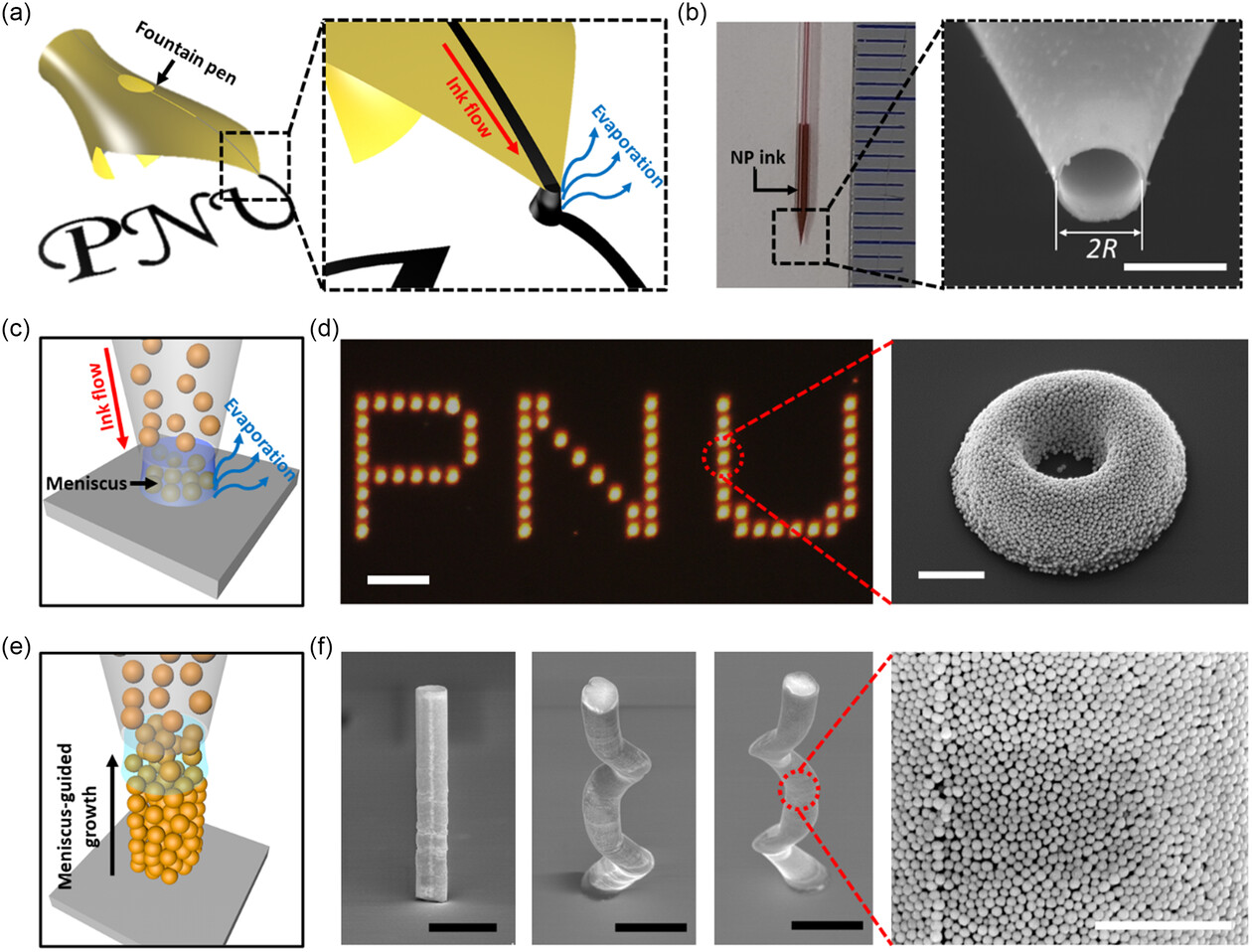 |
| Fountain pen-inspired writing on micrometer scales. a) Scheme of writing using a fountain pen. b) Ultrafine fountain pen for NP dispersed ink. The scale bar represents 5 µμm. c) Scheme of point-like colloidal assembly. d) Micrometer-sized text written by the colloidal assembly (left) and SEM image of a half-donut structure (right). The scale bars of the left and right images represent 50 and 1 µm, respectively. e) Scheme of 3D colloidal assembly. f ) Diverse 3D colloidal assemblies (left) and packing of NP (right). The scale bar represents 10 µm (black) and 1 µm (white). (Reprinted with permission by Wiley-VCH Verlag) |
| The breakthrough allows optical and structural properties of sub-micron pillars to be precisely tuned by mixing particle sizes and nanomaterials. As proof of concept, the researchers demonstrate humidity-responsive NP/biomaterial actuators. This fundamental advance establishes an extremely versatile and accessible platform for designing customized plasmonic metamaterials. |
| This low-cost, high-throughput solution processing technique allows tuning optical properties by mixing particle sizes and materials within a single pillar. The researchers showcase potential applications such as humidity-responsive nanoactuators. The advance establishes an extremely versatile platform to fabricate tailored 3D plasmonic structures for nanophotonics, photocatalysis and nanoscale devices. |
| The key innovation lies in scaling down and reimagining the basic mechanics of an ink pen. At the macroscale, fountain pens rely on wet ink being continuously supplied while the solvent evaporates on paper. The research team designed a tapered glass microcapillary tube that mimics this writing process at the microscopic level. |
| When dipped in colloidal NP ink, the narrow tube tip forms an evaporating capillary bridge just a few microns wide. As the ink self-assembles at this tiny interface, researchers can pull up pillars ranging from hexagonally packed spheres to helical nanostructures. Changing particle concentration in the ink or mixing two different NP solutions enables precise tuning of 3D architectures. |
| For example, combining 80 nm gold NPs (AuNPs) with smaller 20 nm AuNPs significantly boosts maximum pillar height. This happens because the nanoporous assembly allows for capillary rise of fluid within the 3D pillar, increasing the evaporation area for replenishing ink flow. As a result, growth speed is no longer limited by diffusion from the diminishing capillary bridge. |
| The team’s theoretical analysis provides equations relating fabrication parameters like humidity and particle density to experimentally measured pillar expansion rates. This level of quantitative insight will be invaluable for those looking to adapt the technique for specific applications. |
| As a proof of concept, the researchers demonstrated a variety of optical tunability using the NFP. Mixing AuNPs and silver NPs yielded self-assembled half-doughnut shapes with evenly distributed composition. Altering proportions of small and large AuNPs produced pillar nanostructures exhibiting controlled light absorption properties. |
| The team printed asymmetrical “Janus” pillars using NP ink on one side and a functional biological ink containing rod-like M13 bacteriophages on the other. The responsiveness of M13 to humidity gradients induced reversible bending motions, essentially creating miniature humidity-driven actuators out of the two-faced pillars. |
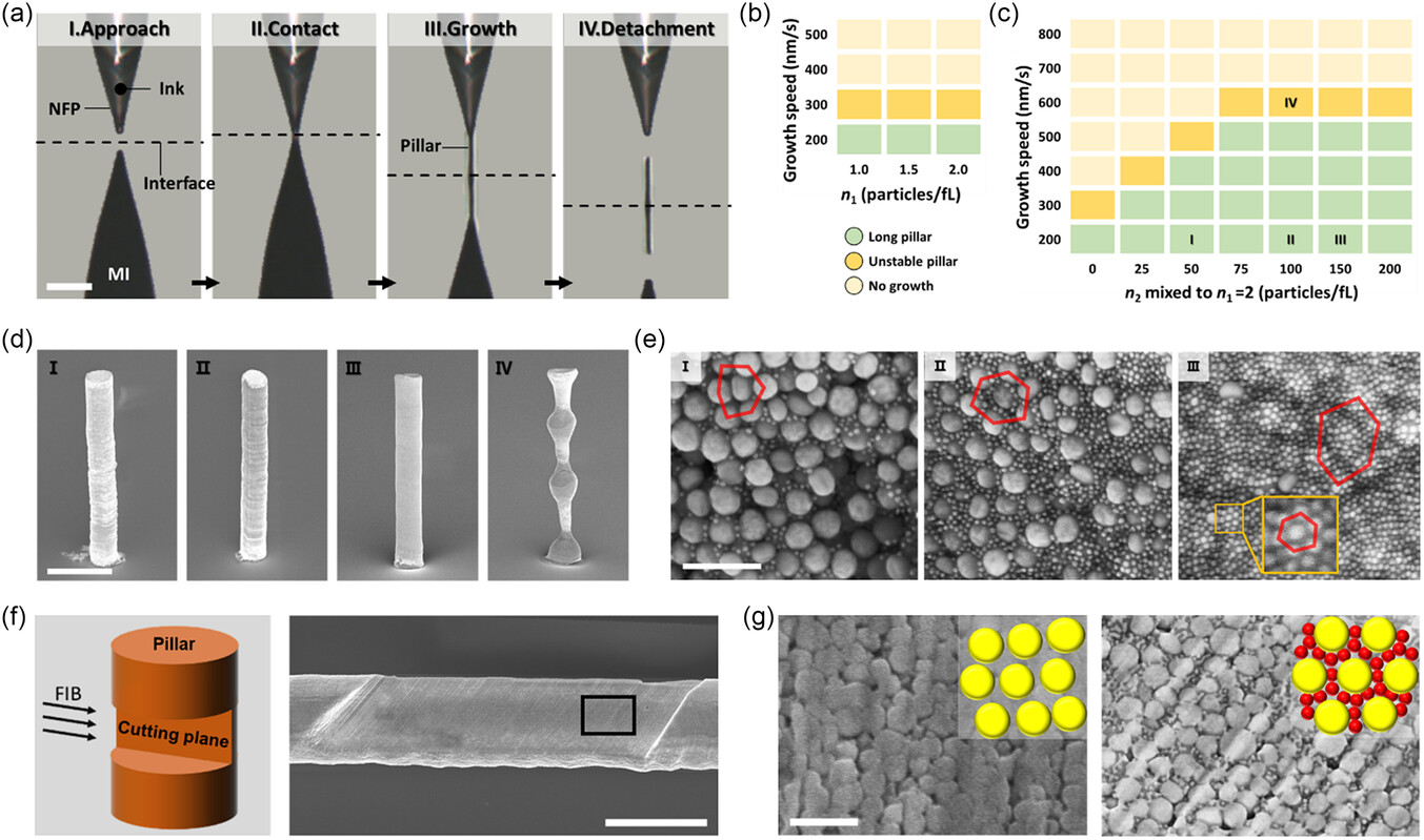 |
| Vertical growth of a binary colloidal cluster. a) Series of optical micrographs showing the vertical growth of the binary colloidal cluster. The scale bar represents 50 µm. b) Available growth speeds based on the 80 nm AuNP solution. c) Available growth speeds based on the 20 nm AuNP solution mixed with 2particles=fL of 80 nm AuNP solution. d) SEM images of the micropillars marked as I, II, III, and IV in (c). The scale bar represents 10 µm. e) SEM images of the nanostructures of micropillars marked as I, II, and III in (d). The scale bar represents 200nm. f ) FESEM image of a micropillar milled with FIB. The scale bar represents 5 µm. g) FESEM image of the cross section of a micropillar composed of a single (left) and binary composition (right). The scale bar represents 200nm. (Reprinted with permission by Wiley-VCH Verlag) |
| This stimulates ideas for manufacturing even more complex colloidal machines by incorporating different nanomaterials, catalysts or proteins within a single 3D-printed pillar. The breadth of possibilities highlights how the researchers’ deceptively simple pen-on-paper concept fundamentally expands the toolkit for advanced nanoengineering. |
| The evaporative fountain pen methodology also circumvents limitations holding back alternative fabrication strategies. Methods reliant on solid–liquid interface gradients can only leverage particle self-assembly in one or two dimensions. More recent template-guided 3D printing approaches have successfully built centimeters-tall plasmonic superlattices. However, they struggle to create small batches of customized pillar designs needed for iterative nanoengineering. |
| There is also a trade-off between pattern complexity and large-scale uniformity since the nanostructures still grow across an extensive evaporation area rather than a confined zone. This leads to practical challenges for efficiently translating lab-based innovation into specialized modules and nanodevices. |
| The reported NFP technique essentially functions as a shrinking 3D printer but with naturally guided rather than externally imposed assembly. Localizing everything to the microscopic interface between surface and pen tip enables exquisite spatiotemporal control without losing scalability. |
| The resulting capacity to continuously alter parameters mid-fabrication and construct heterogeneous pillars less than 10 microns wide unlocks new horizons for rapid nanoprototyping. One can envision scientists designing custom NP structures on the fly to meet performance targets or serve different purposes within an integrated nanosystem. |
| This breakthrough study provides a strong base for many exciting directions. The next phase entails expanding to more nanoparticle types and inks with a wider array of functionalities beyond plasmonics. Researchers must also optimize print speed, architecture stability, and interface sizes to push the boundaries. |
| Another critical task will be investigating alternative substrates since the current reliance on silica wafers poses challenges for integrating nanostructures within devices or onto non-planar surfaces. Finally, exploring reservoir engineering or multi-pen techniques can further broaden tunable compositional complexity for 3D colloidal assembly. |
| The researchers' fountain pen methodology represents a pivotal advancement in nanofabrication, combining the versatile advantages of directed assembly with the scalability of self-assembly. This study essentially transforms an everyday drying pen into a powerful yet accessible nanopatterning platform. |
| The reported technique can serve as an ideal bridge between nanoscience research and real-world technology development. The capacity to test wide-ranging nanostructure compositions and geometries facilitates rapid prototyping to optimize designs for target applications. Meanwhile, the predictable physics confined to a tiny interface allows straightforward scaling up for mass production. |
| Commercial and societal impacts could be profound as researchers exploit the generalizability of this approach across sectors. On the biomedical front, customized 3D nucleic acid nanostructures could enable targeted drug delivery or single cell transfection. Plasmonic pillars with programmable optical resonances could form the basis of ultrasensitive molecular detection platforms. Mix-and-match metamaterials using the technique may lead to enhanced catalytic processes and energy conversion systems. |
| Looking ahead, possibilities abound for incorporating multi-material printing, functional nanoparticle inks, and 3D patterning onto non-planar surfaces – vastly expanding design complexity. If the trend of shrinking transistors adheres to Moore's Law, this discovery of "small thinking" could spur its own paradigm shift – where harnessing standardized nanoscale forces invents endless nano-enabled technologies we cannot yet envision. |
 By
Michael
Berger
– Michael is author of four books by the Royal Society of Chemistry:
Nano-Society: Pushing the Boundaries of Technology (2009),
Nanotechnology: The Future is Tiny (2016),
Nanoengineering: The Skills and Tools Making Technology Invisible (2019), and
Waste not! How Nanotechnologies Can Increase Efficiencies Throughout Society (2025)
Copyright ©
Nanowerk LLC
By
Michael
Berger
– Michael is author of four books by the Royal Society of Chemistry:
Nano-Society: Pushing the Boundaries of Technology (2009),
Nanotechnology: The Future is Tiny (2016),
Nanoengineering: The Skills and Tools Making Technology Invisible (2019), and
Waste not! How Nanotechnologies Can Increase Efficiencies Throughout Society (2025)
Copyright ©
Nanowerk LLC
|

Become a Spotlight guest author! Join our large and growing group of guest contributors. Have you just published a scientific paper or have other exciting developments to share with the nanotechnology community? Here is how to publish on nanowerk.com. |
