

Nanotechnology News – Latest Headlines
ENIAC invites European nanoelectronics players to coordinate "Pilot Line" projects
The ENIAC Joint Undertaking invited the European R+D actors in nanoelectronics to express their interest to coordinate Key Enabling Technologies "Pilot Line" projects underpinning up to 1 billion euros of private and public investments in the next 2 years.
October 23, 2011 Read more

Researchers develop new concept for rechargeable batteries
KIT researchers have developed a new concept for rechargeable batteries. Based on a fluoride shuttle -- the transfer of fluoride anions between the electrodes -- it promises to enhance the storage capacity reached by lithium-ion batteries by several factors.
October 21, 2011 Read more
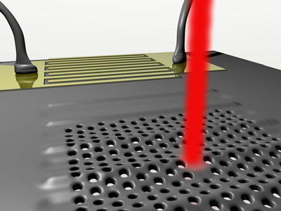
Sound gives nanocavity a twist
Researchers demonstrate that a sound wave can be used to control a photonic crystal.
October 21, 2011 Read more
Laser ion source produces a new generation of semiconductors
For ion implantation, that is 'hammering' ions into the surface layer of the material, conventional ion accelerators are commonly used. Laser ion sources are much simpler, cheaper and more universal. However, they emit wide energy ions usually accompanied by some admixtures. In the Institute of Plasma Physics and Laser Microfusion in Warsaw a unique laser ion source has been built which is equipped with a special system for accelerating ions to a chosen energy and for eliminating admixtures.
October 21, 2011 Read more
Call for papers: China Semiconductor Technology International Conference
CSTIC is the largest annual industrial semiconductor technology conference in China. It is organized by SEMI and ECS, co-organized by China's High-Tech Expert Committee (CHTEC) and co-sponsored by IEEE, MRS and China Electronics Materials Industry Association.
October 21, 2011 Read more
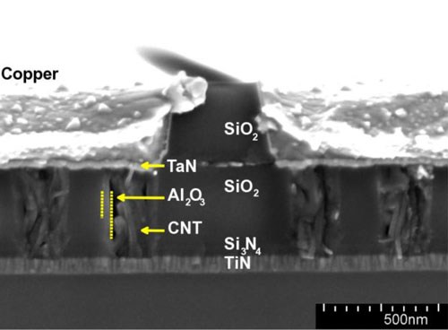
Significant step towards engineering contact modules with vertical carbon nanotube interconnects
Imec researchers, in collaboration with Tokyo Electron, have successfully integrated and characterized carbon nanotubes (CNT) into 150nm contact holes with a TiN underlayer and a Cu single damascene top contact module. The process steps are CMOS-compatible and the platform is designed for fast and automatic electrical testing and for benchmarking different CNT recipes and process conditions.
October 21, 2011 Read more
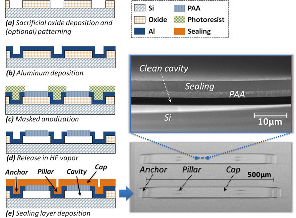
New wafer-level MEMS packaging technology using nanoporous alumina membranes
Imec engineers have, for the first time, demonstrated the fabrication of extremely small sealed cavities (less than one picoliter in volume), fabricated directly on 200mm silicon wafers. The crucial process step is the production of freestanding thin membranes of nanoporous anodic alumina.
October 21, 2011 Read more
Imec uses Si nano-pillar test structures to evaluate advanced cleaning and drying techniques
Imec in collaboration with Lam Research presents a new method for the quantitative evaluation of wafer drying techniques. The method uses Si nano-pillar test structures in combination with top-down scanning electron microscopy (TD-SEM) inspection.
October 21, 2011 Read more
$10m to grow Victoria's small technologies
Minister for Technology Gordon Rich-Phillips has announced a $10 million plan to support Victorian industry to improve productivity through the use of small technologies.
October 21, 2011 Read more
Giant flakes make graphene oxide gel
Rice, Colorado discovery could boost metamaterials, high-strength fibers.
October 21, 2011 Read more
New version of the Archimedes package for semiconductor device simulations has been released
Archimedes is the GNU package for semiconductor device simulations that has been released for the first time in 2005 under GPL. A new version of Archimedes and its GUI has been released on nanoHUB! You can run it on the fly now!
October 20, 2011 Read more

Packard Fellowship to build spectrometer to analyze molecules in 3-D
Junrong Zheng's techniques to see the fine details of how molecules interact have earned the young Rice University scientist a highly prestigious Packard Fellowship.
October 20, 2011 Read more
U.S. government releases environmental, health, and safety research strategy for nanotechnology
The Federal Government today released a national strategy for ensuring that environmental, health, and safety research needs are fully identified and addressed in the fast-growing field of nanotechnology.
October 20, 2011 Read more
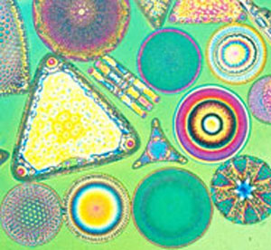
Research grant to learn the secrets of diatoms' nanoscale silica production
Diatoms have found a way of controlling silica at the nanoscale that is very sophisticated and is far beyond what we can achieve in the lab. Learning the secrets of these remarkable cells should enable us to make new catalysts, sensors, diagnostic devices and medical imaging tools.
October 20, 2011 Read more
Responsible development of nanotechnology: Maximizing results while minimizing risk
The U.S. Federal Government is committed to the responsible development of nanotechnology so that the benefits to society are maximized while the potential for unintended consequences from nanomaterials' novel properties is minimized.
October 20, 2011 Read more
Adoption of the new definition of nanomaterials by the European Commission: first reactions and analyses
This Tuesday, October 18, the European Commission published its long-awaited definition of nanomaterials after a year of intense negotiations. The reactions were not long in coming, revealing power struggles so far mainly confined to Brussels area. Here is a first insight into the politics hidden behind this supposedly neutral and "scientific" definition, the next obstacles and important meetings.
October 20, 2011 Read more
 Subscribe to our Nanotechnology News feed