Atomic Layer Etching: Precise Nanoscale Material Removal
What is Atomic Layer Etching?
Atomic layer etching (ALE) is a highly controlled and selective etching technique that removes material layer by layer at the atomic scale. It is a cyclic process that relies on self-limiting chemical reactions to achieve precise material removal with atomic-level accuracy. ALE has emerged as a crucial technology for advanced nanofabrication, enabling the creation of ultra-thin films, high-aspect-ratio structures, and complex 3D architectures.
Key Principles of Atomic Layer Etching
Atomic layer etching operates on several key principles that distinguish it from conventional etching techniques:
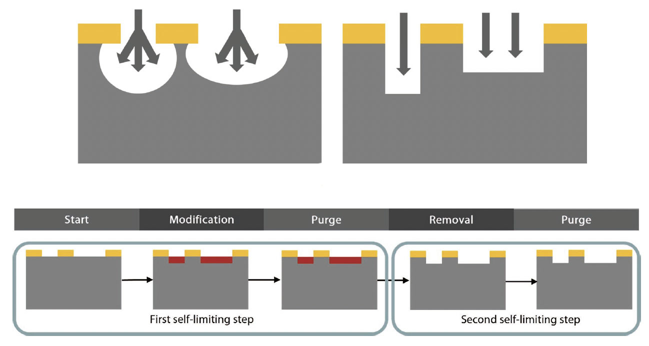
- Self-Limiting Reactions: ALE relies on self-limiting chemical reactions that inherently limit the etching process to a single atomic layer per cycle. Once the surface layer is modified or etched, the reaction stops, preventing further etching until the next cycle begins.
- Separation of Surface Modification and Etching: ALE separates the surface modification step from the etching step, allowing for precise control over the etching process. The surface modification step prepares the surface layer for removal, while the etching step selectively removes the modified layer.
- Atomic-Level Precision: By controlling the number of etching cycles, ALE enables the removal of material with atomic-level precision. This level of control is crucial for fabricating ultra-thin films, high-aspect-ratio structures, and complex 3D architectures.
- Material Selectivity: ALE can achieve high material selectivity by exploiting differences in the chemical reactivity of different materials. By carefully selecting the reactive species and etching conditions, ALE can selectively etch one material while leaving others intact.
ALE Process Steps
The atomic layer etching process typically consists of two main steps that are repeated in a cyclic manner:
- Surface Modification: In this step, a reactive species, such as a gas or plasma, is introduced into the etching chamber. The reactive species chemically modifies the surface layer of the material, creating a modified layer that is more susceptible to etching. This step is self-limiting, as the reaction stops once the surface layer is completely modified.
- Etching: After the surface modification step, the modified layer is selectively removed using an etchant. The etchant can be a different reactive species, such as a gas, plasma, or ion beam. The etching step is also self-limiting, as it stops once the modified layer is completely removed, exposing the underlying unmodified material.
These two steps are repeated in a cyclic manner until the desired amount of material is etched. By controlling the number of cycles, the depth of the etched material can be precisely controlled at the atomic scale.
Etching Directionality: Isotropic vs. Anisotropic Etching
Atomic layer etching can be classified into two main categories based on the directionality of the etching process: isotropic etching and anisotropic etching.
Isotropic Etching
Isotropic etching is a type of etching where the material is removed uniformly in all directions. In isotropic ALE, the etching rate is equal in both the vertical and lateral directions, resulting in a rounded or undercut etch profile. Isotropic etching is useful for creating structures with smooth, curved surfaces or for removing material from hard-to-reach areas.
Anisotropic Etching
Anisotropic etching, on the other hand, is a type of etching where the material is removed preferentially in one direction. In anisotropic ALE, the etching rate is higher in the vertical direction than in the lateral direction, resulting in a more directional etch profile with steep sidewalls. Anisotropic etching is crucial for creating high-aspect-ratio structures, such as deep trenches, vertical fins, or nanoscale pillars.
The choice between isotropic and anisotropic etching depends on the specific application and the desired structure. In some cases, a combination of both etching modes may be employed to achieve the optimal etch profile. The ability to control the etching directionality is one of the key advantages of atomic layer etching, enabling the fabrication of a wide range of nanoscale structures with precise geometries.
Advantages of Atomic Layer Etching
Atomic layer etching offers several key advantages over conventional etching techniques:
- Atomic-Level Control: ALE enables precise control over the etching depth with atomic-level accuracy. This level of control is essential for fabricating ultra-thin films, high-aspect-ratio structures, and complex 3D architectures.
- High Selectivity: ALE can achieve high material selectivity by exploiting differences in the chemical reactivity of different materials. This selectivity allows for the etching of one material while leaving others intact, enabling the creation of complex, multi-material structures.
- Reduced Damage: ALE is a gentler etching process compared to conventional techniques, as it relies on chemical reactions rather than physical bombardment. This reduces the risk of damage to the underlying material, preserving its structural and electronic properties.
- Conformal Etching: ALE can achieve conformal etching of complex 3D structures, as the self-limiting nature of the process ensures uniform etching across the entire surface. This is particularly important for high-aspect-ratio structures and advanced nanoscale devices.
Applications of Atomic Layer Etching
Atomic layer etching has a wide range of applications in nanofabrication and advanced manufacturing:
- Semiconductor Manufacturing: ALE is used in the fabrication of advanced semiconductor devices, such as transistors, memory cells, and photonic structures. It enables the creation of ultra-thin gate oxides, high-aspect-ratio fins, and complex 3D architectures that are crucial for the continued scaling of semiconductor technology.
- Nanophotonics: ALE is employed in the fabrication of nanophotonic devices, such as waveguides, resonators, and photonic crystals. The precise control over etching depth and selectivity offered by ALE is essential for creating high-quality optical structures with low losses and high performance.
- MEMS and NEMS: ALE is used in the fabrication of micro- and nanoelectromechanical systems (MEMS and NEMS), such as sensors, actuators, and resonators. The ability to precisely etch complex 3D structures with high aspect ratios is crucial for the development of advanced MEMS and NEMS devices.
- Quantum Devices: ALE is employed in the fabrication of quantum devices, such as quantum dots, nanowires, and superconducting circuits. The atomic-level control and high selectivity offered by ALE are essential for creating the precise, nanoscale structures required for quantum applications.
Challenges and Future Perspectives
Despite the many advantages of atomic layer etching, there are still challenges to be addressed for its widespread adoption in industrial manufacturing. One of the main challenges is the relatively low etching rate compared to conventional techniques, which can limit throughput and productivity. Researchers are working on developing faster ALE processes that can maintain the atomic-level precision while increasing the etching rate.
Another challenge is the development of new chemistries and reactive species for ALE. While ALE has been demonstrated for a range of materials, including semiconductors, dielectrics, and metals, there is a need for expanded material compatibility and selectivity. The discovery and optimization of novel ALE chemistries will be crucial for enabling the etching of a wider range of materials and structures.
In the future, atomic layer etching is expected to play an increasingly important role in the fabrication of advanced nanoscale devices. The integration of ALE with other nanofabrication techniques, such as atomic layer deposition (ALD) and nanoimprint lithography, will enable the creation of complex, multi-material structures with unprecedented precision and functionality. Additionally, the development of in-situ monitoring and control techniques for ALE will further enhance the reliability and reproducibility of the etching process.
Further Reading
The Journal of Physical Chemistry Letters, Atomic Layer Etching: Rethinking the Art of Etch
Journal of Vacuum Science & Technology A, Thermal atomic layer etching: A review
Accounts of Chemical Research, Mechanisms of Thermal Atomic Layer Etching
