Photonic Bandgap: Physics, Structure, Fabrication, and Applications
What Is a Photonic Bandgap?
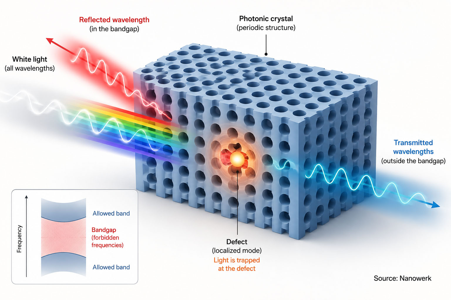
In one sentence: A photonic bandgap is a range of electromagnetic frequencies that cannot propagate through a periodically structured dielectric material, the optical analog of the energy bandgap that forbids certain electron states in a semiconductor.
A photonic bandgap is the defining property of a photonic crystal, an artificial material whose refractive index is modulated periodically on a length scale comparable to the wavelength of light, typically a few hundred nanometers in the visible and near infrared. Inside the gap, light is reflected by the structure rather than transmitted, and in the special case of a complete bandgap the rejection is omnidirectional and independent of polarization. Photonic crystals behave for photons in much the way that a semiconductor behaves for electrons: certain energies are allowed and certain energies are forbidden, with the analogy formalized by treating the dispersion of light in a periodic dielectric as a band structure and the analog of the electronic bandgap as a photonic one.
Common misconception: A photonic bandgap does not mean the material absorbs those colors of light. In an ideal low-loss photonic crystal, frequencies inside the gap are reflected or confined because propagating optical modes are unavailable.
The concept was proposed independently in 1987 by Eli Yablonovitch and Sajeev John. Yablonovitch was interested in inhibiting spontaneous emission to improve semiconductor lasers and solar cells, while John was studying the localization of photons by analogy with electron localization in disordered solids; both papers concluded that a three-dimensional dielectric structure with sufficient index contrast and the right symmetry could possess an omnidirectional photonic bandgap. The first three-dimensional structure to demonstrate such a gap was machined into a high-index dielectric in 1991 by drilling three sets of crossed holes and became known as Yablonovite. Photonic bandgap phenomena also occur in nature: the iridescence of natural opals, peacock feathers, and several butterfly species arises from partial photonic bandgaps in biological microstructures with sub-micrometer periodicity, producing what is now called structural color.
Key takeaways:
- A photonic bandgap is a range of optical frequencies forbidden from propagating through a periodic dielectric structure.
- The effect arises from coherent Bragg scattering and is mathematically analogous to the electronic bandgap of a semiconductor.
- Photonic bandgaps can be one, two, or three dimensional, with a complete three-dimensional bandgap usually requiring high refractive-index contrast, often of order 2:1 or greater, depending on geometry and filling fraction.
- Deliberate defects in a photonic bandgap structure create high-quality resonant cavities and low-loss waveguides that underpin photonic crystal lasers, fibers, and integrated nanophotonic circuits.
Underlying Physics: Bragg Scattering and Photonic Band Structure
When light passes through a medium whose refractive index varies periodically on a length scale comparable to roughly half the wavelength in the material, partial reflections at each interface can interfere constructively for some frequencies and destructively for others. For a one-dimensional stack of alternating high- and low-index layers, this is the familiar Bragg-mirror stopband. Extending the periodicity to two or three dimensions, with the right symmetry and index contrast, opens a range of frequencies for which propagating modes are forbidden in every direction simultaneously, a complete photonic bandgap.
Strictly, a bandgap forbids propagating Bloch modes in an ideal infinite periodic structure. In real finite structures, the same physics appears as a strong reflection or transmission stopband rather than perfect rejection, because finite size, disorder, absorption, tunneling, and out-of-plane leakage can allow some residual transmission or loss.
The mathematics parallels electronic band-gap engineering. The propagation of light in a periodic dielectric is described by Bloch states characterized by a frequency ω and a wave vector k inside the first Brillouin zone, obtained by solving Maxwell's equations under periodic boundary conditions. The resulting photonic band structure is a set of dispersion curves ω(k); a complete bandgap exists when two consecutive bands do not overlap in any direction. The two bands bordering the gap are often called the dielectric band and the air band, because the lower-band field concentrates in the high-index regions while the upper-band field concentrates in the low-index regions, a feature that has important consequences for how defects modify the spectrum.
The width and position of a photonic bandgap depend on three quantities: the refractive index contrast between the constituent materials, the geometry and symmetry of the periodic lattice, and the volume fraction of each material. A complete three-dimensional bandgap in a dielectric structure usually requires high refractive-index contrast, often of order 2:1 or greater, though the exact threshold depends on lattice symmetry, topology, and filling fraction. Silicon (n ≈ 3.5) in air comfortably exceeds this range, while silica (n ≈ 1.45) in air usually does not. Diamond-like lattices and woodpile structures are classic geometries for wide complete gaps, while inverse opals are an experimentally important route to three-dimensional photonic crystals and can support stopbands or complete gaps under suitable conditions.
One-, Two-, and Three-Dimensional Photonic Bandgaps
Photonic bandgaps differ qualitatively depending on the number of dimensions in which the dielectric is periodic. A one-dimensional photonic bandgap is the stopband of a distributed Bragg reflector, in which alternating high- and low-index layers reflect a band of wavelengths near normal incidence. A two-dimensional photonic bandgap arises in an array of parallel rods, holes, or pillars patterned periodically in a plane, and a three-dimensional photonic bandgap is the complete omnidirectional gap originally envisioned by Yablonovitch and John.
| Dimensionality | Typical structure | Light confinement | Main fabrication route | Representative uses |
|---|---|---|---|---|
| 1D photonic bandgap | Multilayer Bragg stack, distributed Bragg reflector | Along one axis, at near-normal incidence | Thin-film deposition, chemical vapor deposition | Laser mirrors, antireflection coatings, VCSELs |
| 2D photonic bandgap | Photonic crystal slab with periodic holes or pillars; photonic bandgap fiber cladding | In the plane of periodicity; total internal reflection out of plane | Electron-beam lithography plus reactive-ion etching; stack-and-draw fiber processing | Photonic crystal waveguides and cavities, hollow-core fibers, integrated photonic chips |
| 3D photonic bandgap | Yablonovite, woodpile structure, inverse opal | Omnidirectional, all polarizations | Layer-by-layer assembly, colloidal colloidal templating, two-photon direct laser writing | Spontaneous-emission control, full 3D optical confinement, fundamental studies of light localization |
Two-dimensional photonic crystal slabs combine the in-plane bandgap of a periodic hole array with vertical confinement by total internal reflection in a thin high-index membrane, typically silicon on insulator. They have become the workhorse platform of integrated nanophotonics because they are compatible with planar CMOS-style fabrication and yet can support resonances with quality factors exceeding 106. Three-dimensional photonic crystals are scientifically the cleanest realization of the original concept but remain much harder to fabricate at visible and near-infrared wavelengths, which is why the bulk of device-level work today uses 1D and 2D structures.
Useful Terminology
| Term | Meaning |
|---|---|
| Photonic crystal | A periodic dielectric structure that controls light through interference and photonic band formation. |
| Photonic bandgap | A forbidden optical frequency range in which propagating modes are unavailable in one or more directions. |
| Stopband | A directional reflection band, especially common in one-dimensional Bragg stacks. |
| Complete bandgap | A gap in which propagation is forbidden for all directions and polarizations in an ideal infinite structure. |
| Defect mode | A localized allowed mode intentionally introduced inside the forbidden gap by disrupting the periodic lattice. |
Defect Modes and Why the Bandgap Becomes Useful
A pristine photonic bandgap rejects light, but the technologically interesting devices are made by deliberately disrupting the periodicity. Removing or modifying a unit cell creates a defect mode whose frequency falls inside the bandgap, in close analogy with dopant states inside the electronic bandgap of a semiconductor. Because nothing else can propagate at that frequency, the mode is trapped at the defect with minimal radiation loss.
Point defects act as optical cavities with extremely small mode volumes, often well below one cubic wavelength, while supporting high quality factors. Line defects act as photonic crystal waveguides that can carry light around compact bends with reduced radiative loss when the bend and mode matching are carefully designed, because light at the guided frequency cannot easily escape into the surrounding bandgap material. Coupled defects form arrays of resonators that produce flat bands and slow-light propagation. Together, point and line defects support the photonic equivalent of an integrated circuit on a chip, with quality factors in dielectric slab cavities now routinely exceeding 105 to 106.
How Photonic Bandgap Structures Are Made
Operation at visible and near-infrared wavelengths requires sub-micrometer periodicity, which places photonic bandgap fabrication firmly within nanofabrication. For 2D slabs, electron-beam lithography followed by reactive-ion etching of silicon-on-insulator membranes is the standard research approach, producing hole arrays with single-nanometer dimensional control, while deep-ultraviolet and immersion photolithography are extending these structures into industrial silicon photonics lines. For 3D structures, three families of route are common: layer-by-layer stacking of patterned dielectric layers to build woodpile lattices, self-assembly of colloidal silica or polystyrene spheres into opals followed by infiltration with a high-index medium such as silicon or titania and template removal to yield inverse opals, and two-photon direct laser writing into a photoresist to produce arbitrary 3D architectures with sub-micrometer features.
Photonic bandgap fibers are made by stacking glass capillaries into a periodic preform and drawing the assembly under heat, preserving the geometry over kilometers of fiber. A missing capillary defines an air core surrounded by a periodic silica cladding, producing a hollow-core photonic bandgap fiber. One-dimensional photonic bandgap structures, by contrast, are deposited by physical or chemical vapor deposition of alternating dielectric layers.
Limitations and Practical Challenges
Photonic bandgap devices are highly sensitive to fabrication disorder because their operation depends on interference over many unit cells. Sidewall roughness, dimensional errors, absorption, and finite-size leakage can reduce the quality factor of cavities, increase waveguide loss, or shift the bandgap away from the design wavelength.
Complete three-dimensional bandgaps remain especially difficult to realize at visible and near-infrared wavelengths because they require high-index materials, accurate 3D nanofabrication, low optical absorption, and enough unit cells to approximate the ideal infinite lattice.
Applications
Photonic bandgap fibers and fiber optics
A hollow-core photonic bandgap fiber guides nearly all of its optical power in air rather than glass, drastically lowering the optical nonlinearity, raising the damage threshold, and reducing the propagation latency by about 30 percent relative to a conventional silica fiber. Single-mode photonic bandgap guidance of light in air was first demonstrated in 1999, and modern hollow-core fibers, including both photonic-bandgap and antiresonant designs, have reached losses approaching those of solid silica fiber at telecommunications wavelengths. Applications include high-power laser delivery, gas-cell spectroscopy, mid-infrared transmission beyond the absorption window of silica, ultra-low-latency data links, and pulse compression in ultrafast laser systems.
Photonic crystal lasers and light sources
A defect cavity inside a 2D photonic crystal slab combines a small mode volume with a high quality factor, enabling ultra-low-threshold semiconductor lasers and efficient single-photon sources. Because the photonic bandgap modifies the local density of optical states, an emitter placed near a band edge or inside a defect cavity can radiate orders of magnitude faster than in free space through the Purcell effect, while an emitter placed in the bulk of a complete 3D bandgap is inhibited from radiating at the gap frequency because no electromagnetic modes exist to couple to. Both regimes are central to nanolasers, bright single-photon emitters, and efficient solid-state light sources.
Integrated nanophotonics and slow light
Slab photonic crystals are used to route, filter, split, and modulate light at high density on silicon chips, an architecture central to nanophotonic circuits. Engineering a flat region of a photonic band near the bandgap edge produces a slow-light regime in which the group velocity drops by one to two orders of magnitude, enhancing nonlinear interactions and shrinking the footprint of phase-sensitive devices such as switches and modulators. Photonic-crystal cavities coupled to quantum dots or solid-state color centers serve as building blocks for quantum photonics platforms.
Structural color and sensing
Partial photonic bandgaps in low-contrast structures produce angle-dependent reflection bands that the eye perceives as structural color. Engineered opals and inverse opals are used as non-fading pigments, anti-counterfeiting features, and optical sensors in which a small change in the lattice spacing, induced by mechanical strain, chemical swelling, or analyte binding, shifts the reflection peak by a measurable amount. Tunable optical materials built around responsive photonic crystals are an active research area for displays, wearable sensors, and dynamic surfaces.
Current Research Directions
Topological photonic crystals are an active extension of photonic bandgap physics. In simple terms, these approaches use the band structure not only to block light, but also to create protected pathways for optical signals. Engineering symmetry-protected band crossings or band inversions inside the bandgap creates topologically nontrivial edge states that can propagate around defects and sharp bends with strongly reduced back-reflection. Robustness against fabrication disorder makes such edge states attractive for waveguides, lasers, and quantum-optical interconnects, with platforms ranging from all-dielectric photonic crystals to metamaterials and coupled microring arrays.
Inverse design has changed how photonic bandgap structures are conceived. Instead of starting from an intuitive lattice, gradient-based or topology-optimization algorithms search the design space for structures that maximize an arbitrary figure of merit, such as bandgap width, cavity quality factor, mode volume, or filter response, under fabrication constraints. The resulting devices often look freeform and counterintuitive but routinely outperform hand-designed lattices in both simulation and experiment. Hybrid platforms that combine photonic bandgap confinement with plasmonic, polaritonic, or phononic elements, including phononic crystals and optomechanical crystals, are being developed to combine the strengths of multiple wave systems on a single chip.
FAQ: Photonic Bandgap
What is the difference between a photonic bandgap and an electronic bandgap?
Both arise from waves traveling through a periodic potential, but the wave and the potential are different. An electronic bandgap is a range of energies forbidden to electrons in the periodic atomic potential of a crystal. A photonic bandgap is a range of frequencies forbidden to electromagnetic waves in a periodic dielectric structure whose length scale matches the wavelength of light, typically hundreds of nanometers in the visible and near infrared. The mathematics is closely analogous, but the photonic case is governed by Maxwell's equations rather than the Schrödinger equation, and the relevant periodicity is engineered rather than atomic.
Does every photonic crystal have a complete photonic bandgap?
No. Most photonic crystals have only partial or directional bandgaps, meaning that propagation is forbidden along certain symmetry directions but allowed along others. A complete bandgap, in which light is forbidden in every direction and for every polarization, requires a sufficiently high refractive index contrast, often of order 2:1 or greater, together with the right lattice symmetry and filling fraction. The exact threshold depends on lattice topology and material filling fraction. Diamond-like lattices and woodpile structures are classic geometries for wide complete gaps, while inverse opals are experimentally important three-dimensional photonic crystals that can support stopbands or complete gaps under suitable conditions.
Why do photonic bandgap fibers guide light in air?
Conventional optical fibers guide light by total internal reflection in a higher-index glass core surrounded by a lower-index cladding. A photonic bandgap fiber instead surrounds a hollow air core with a microstructured periodic cladding that supports a photonic bandgap at the operating wavelength. Light at frequencies inside the bandgap cannot propagate into the cladding and is therefore confined to the air core, even though air has a lower refractive index than the surrounding glass. Hollow-core operation reduces nonlinearity, lowers latency, and raises damage thresholds compared with solid-core fibers.
How is a photonic crystal cavity different from a Fabry–Perot cavity?
A Fabry–Perot cavity confines light between two distant mirrors, typically over a mode volume of many cubic wavelengths. A photonic crystal cavity confines light at a localized defect inside a photonic bandgap material, with no propagating modes available at the resonant frequency in any direction around the defect. The result is a much smaller mode volume, often below one cubic wavelength, while still achieving quality factors of 104 to over 106. The small mode volume strongly enhances light–matter interactions, which is exploited in low-threshold lasers and single-photon sources.
Why does the refractive index contrast matter so much?
The size of a photonic bandgap scales with the strength of the periodic modulation of the dielectric constant. A higher refractive index contrast produces stronger Bragg scattering at each interface, which in turn opens a wider gap between the lower and upper photonic bands. For two-dimensional and three-dimensional structures, low contrast may only produce directional gaps, while a contrast of order 2:1 or greater is often needed for a complete bandgap, depending on lattice symmetry, topology, and filling fraction. Silicon in air, with an index ratio near 3.5, is a common high-contrast platform, while silica in air is usually too low in contrast to give a complete gap.
Further Reading
Physical Review Letters, Inhibited Spontaneous Emission in Solid-State Physics and Electronics
Physical Review Letters, Strong Localization of Photons in Certain Disordered Dielectric Superlattices
Nature Communications, Topological photonics: robustness and beyond
