| Feb 13, 2020 |
New etching technique could advance the way semiconductor devices are made(Nanowerk News) Microelectronics like semiconductor devices are at the heart of the technologies we use each day. As we move into an era where we are stretching the limits of Moore’s Law, it is essential to find new ways to continue to pack more circuitry into each individual device in order to increase the speed and capability of our computers. |
| Researchers at the U.S. Department of Energy’s (DOE) Argonne National Laboratory have developed a new technique that could potentially help make these increasingly small but complex devices. The technique, known as molecular layer etching, is detailed in a paper published in Chemistry of Materials ("Molecular Layer Etching of Metalcone Films Using Lithium Organic Salts and Trimethylaluminum"). |
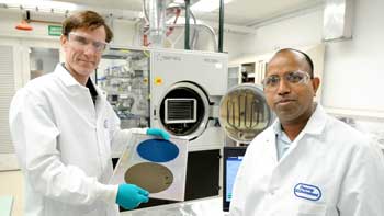 |
| Argonne chemists Jeff Elam (left) and Anil Mane (right) and colleagues have molecular layer etching that may help develop microelectronics and show the way beyond Moore’s Law. Not shown are Matthias Young, Angel Yanguas-Gil, Devika Choudhury and Steven Letourneau. (Image: Argonne National Laboratory) |
| To make microelectronics smaller, manufacturers have to cram in more and more circuitry onto smaller films and 3D structures. Today, this happens by using thin film deposition and etching, techniques to grow or remove films one layer at a time. |
| “Our ability to control matter at the nanoscale is limited by the kinds of tools we have to add or remove thin layers of material. Molecular layer etching (MLE) is a tool to allow manufacturers and researchers to precisely control the way thin materials, at microscopic and nanoscales, are removed,” said lead author Matthias Young, an assistant professor at the University of Missouri and former postdoctoral researcher at Argonne. |
| Together with molecular layer deposition (MLD), a deposition technique, MLE can be used to design microscopic architectures. These approaches are analogs of atomic layer deposition (ALD) and atomic layer etching (ALE), the more commonly applied techniques for fabricating microelectronics. However, unlike atomic layering techniques, which deal exclusively with inorganic films, MLD and MLE can be used to grow and remove organic films as well. |
How it works |
| In principle, MLE works by exposing thin films, several nanometers or micrometers thick, to pulses of gas inside a vacuum chamber. The process starts with one gas (Gas A) which, upon entry, reacts with the surface of the film. Next, the film is exposed to a second gas (Gas B). This AB process is repeated until the desired thickness is removed from the film. |
| “The net effect of A and then B is the removal of a molecular layer from your film,” said Argonne chemist Jeff Elam, a co-author of the study. “If you do that process sequentially, over and over again, you can reduce the thickness of your film to achieve the desired final thickness.” |
| A key aspect of MLD is that the A and B surface reactions are self-limiting. They only continue until all of the available reactive surface sites are consumed, and then the reactions naturally terminate. This self-limiting behavior is extremely helpful in manufacturing since it is relatively easy to scale the process up to larger substrate sizes. |
| Researchers tested their approach using alucone, an organic material similar to silicone rubber that has potential applications in flexible electronics. Gas A in their experiment was a lithium-containing salt, and Gas B was trimethyl aluminum (TMA), an organometallic aluminum-based compound. |
| During the etching process, the lithium compound reacted with the surface of the alucone film in a way that caused the lithium to stick onto the surface and disrupt the chemical bonding in the film. Then, when the TMA was introduced and reacted, it removed the layer of film containing lithium. The lithium serves a sacrificial role — it is deposited on the surface temporarily to break chemical bonds but is then removed by the TMA. |
| “The process can go on layer by layer like that and you can remove the whole material if you wanted to,” Young said. |
Opening new doors in microelectronics |
| Using this technique can help manufacturers and researchers develop new ways of making nanostructures. The process may also be a safer option for them to use because it is free of halogens, a harsh components of chemicals common in other etching processes. It also has the advantage of being selective; the etching technique can selectively remove MLD layers without affecting nearby ALD layers. |
| “MLE has the potential to help usher in new pathways for fabricating and controlling material geometries at the nanoscale, which could open new doors in microelectronics and extend beyond traditional Moore’s Law scaling,” Elam said. |
| Source: Argonne National Laboratory |
|
Subscribe to a free copy of one of our daily Nanowerk Newsletter Email Digests with a compilation of all of the day's news. |

