| Oct 28, 2021 |
Stacking the deck - Layers of crystalline nanosheets enable tunable electronic properties
(Nanowerk News) Boron is a versatile non-metal element, but until the last five years, chemists have only theorized about the useful properties and applications of two-dimensional (2D) boron-containing materials.
|
|
In a study published this month in the Journal of Materials Chemistry A ("Crystalline boron monosulfide nanosheets with tunable bandgaps"), a group led by researchers from the University of Tsukuba brought theory to life by preparing the first 2D boron monosulfide (BS) nanosheets, which can be handled layer-by-layer to control their electronic properties.
|
|
The inherently large surface areas and diverse electronic states of 2D materials make them good candidates for applications in batteries and other devices. Moreover, combining 2D building blocks into novel materials can allow for greater control over their functionalities. Previous computational studies had suggested that BS in particular could adopt several stable 2D structures with unique properties.
|
|
Therefore, the researchers fabricated a 1:1 boron:sulfide bulk material, which had a rhombohedral (a three-dimensional rhombus) crystal structure (r-BS), and then stripped away individual nanolayers (2D BS), which maintained the original material’s crystalline arrangement.
|
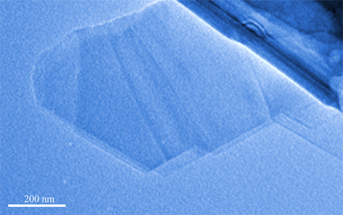 |
| Researchers obtain boron monosulfide nanosheets for the first time and demonstrate unique electronic functionality that can be controlled by changing the number of layers in the stack. (Image: University of Tsukuba)
|
|
“Our analysis confirmed what our own calculations had predicted,” says research group leader, Professor Takahiro Kondo. “That is, BS nanosheets had a different bandgap energy than the bulk material, and importantly, the bandgap could be tuned based on the number of stacked 2D BS sheets.”
|
|
The bandgap energy of a material is related to its ability to conduct an electrical current, and it is therefore a key property linked to potential electronic device applications. The researchers found that the bandgap energy of a single BS nanosheet was relatively large, but it decreased successively as they added one or two additional nanosheet layers. The bandgap energy of the stack ultimately reached the level of the bulk r-BS after about five sheets were assembled.
|
|
“This feature and light effective-electron-mass of the BS nanosheets indicated that they could potentially serve as n-type semiconductor materials with high conductivity,” explains Prof. Kondo, “which makes them unique among other known 2D boron-containing materials that do not have bandgaps.”
|
|
Because of their distinct bandgap structures, electrodes comprising r-BS or 2D BS responded to different wavelengths of light. The r-BS required lower-energy irradiation (i.e., visible light) to conduct a current and exhibit photocatalytic behavior, whereas the larger bandgap of the 2D BS was only active under higher-energy ultraviolet light.
|
|
Indeed, boron is far from boring! These light-induced phenomena highlighted the fact that 2D boron monosulfide materials can be applied in photocatalytic or electronic devices, and importantly, their properties can be tuned as needed by controlling the number of nanosheets.
|

