| Mar 19, 2022 |
New technique opens door to cheaper semiconductors, higher chip yield(Nanowerk News) Scientists from the NTU Singapore and the Korea Institute of Machinery & Materials (KIMM) have developed a technique to create a highly uniform and scalable semiconductor wafer, paving the way to higher chip yield and more cost-efficient semiconductors. |
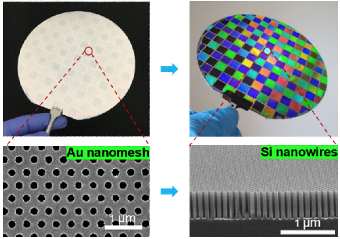 |
| Left: Image of a six-inch silicon wafer with printed metal layers and its top-view scanning electron microscope image. Right: Image of the six-inch silicon wafer with nanowires and its cross-sectional scanning electron microscope image. (Image: NTU Singpore) |
| Semiconductor chips commonly found in smart phones and computers are difficult and complex to make, requiring highly advanced machines and special environments to manufacture. |
| Their fabrication is typically done on silicon wafers and then diced into the small chips that are used in devices. However, the process is imperfect and not all chips from the same wafer work or operate as desired. These defective chips are discarded, lowering semiconductor yield while increasing production cost. |
| The ability to produce uniform wafers at the desired thickness is the most important factor in ensuring that every chip fabricated on the same wafer performs correctly. |
| Nanotransfer-based printing– a process that uses a polymer mould to print metal onto a substrate through pressure, or ‘stamping’ – has gained traction in recent years as a promising technology for its simplicity, relative cost-effectiveness, and high throughput. |
| However, the technique uses a chemical adhesive layer, which causes negative effects, such as surface defects and performance degradation when printed at scale, as well as human health hazards. For these reasons, mass adoption of the technology and consequent chip application in devices has been limited. |
| In their study, which was published in the peer-reviewed journal ACS Nano ("Direct Chemisorption-Assisted Nanotransfer Printing with Wafer-Scale Uniformity and Controllability"), the research team from NTU and KIMM reported that their chemical-free printing technique, when combined with metal-assisted chemical etching – a method used to enhance the contrast on surfaces to make nanostructures visible - resulted in semiconductor wafers with nanowires (nanostructures in cylindrical form) that were highly uniform and scalable. |
| The semiconductor also demonstrated better performance when compared with current chips in the market. Moreover, the fabrication method is also fast and leads to high chip yield. |
| Source: Nanyang Technological University |

