| Dec 23, 2011 |
Imaging electrons by the slice |
| (Nanowerk News) Understanding and visualizing the energy states of electrons in a crystal provides important insights into many modern electronic materials, such as superconductors, or other materials that physicists can use to develop novel electronic applications. The electronic states at the surface of a crystal, or the two-dimensional layers within a sample, are of particular interest to materials scientists, but are notoriously difficult to image using conventional techniques. |
| Now, a technique is available to measure two-dimensional electronic states within a crystal (see paper in Physical Review Letters: "Common Origin of the Circular-Dichroism Pattern in Angle-Resolved Photoemission Spectroscopy of SrTiO3 and CuxBi2Se3"). The technique was developed by researchers at the RIKEN SPring-8 Center, Harima, along with colleagues from the University of Tokyo and several other institutes in Japan, China and the USA. The technique enables in-depth study of these two-dimensional electronic states for the first time (Fig. 1). Many of the materials of greatest interest for novel electronic applications are based on the intricate properties of such electronic states, explains team member Yukiaki Ishida. |
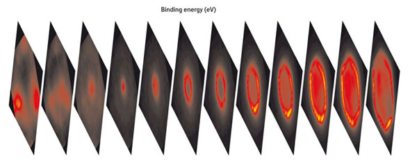 |
| Figure 1: The electronic states at the surface of the topological insulator CuxBi2Se3, which can now be measured. The vertical axis shows the electron energy, the horizontal axes depict the electron momentum in the two-dimensional plane. |
| One of the most widely used techniques to image a material's electronic states is called angle-resolved photoemission spectroscopy (ARPES). Using this technique, physicists shine a light beam on a crystal and then record the pattern of the photoelectrons that are ejected from the crystal's surface. When they use laser beams of different polarization, they can obtain further important details of the electronic states of the crystal. |
| When studying ARPES measurements made on two different crystals—SrTiO3:Nb and CuxBi2Se3—Ishida and colleagues discovered that, under some experimental circumstances, there is a common pattern in the photoelectron distribution that is also known as the 'pattern of photoemission'. The catch is that this pattern occurs only when the two-dimensional electronic states probed therein are thin enough. |
| This technique can provide unique insight into a number of widely studied materials. High-temperature superconductors, for example, are made of thin atomic layers that are crucial to their superconductivity. A recently discovered class of materials, topological insulators, also has promising properties: the electrons of these materials can travel at their surface almost without any losses to the orientation of the electron's magnetic property, which has potential application in new ways of computing. |
| Beyond the study of novel electronic materials, studying the surfaces of materials may reveal new findings, says Ishida. "How surface states change during catalytic reactions is of major scientific and commercial interest," he explains. "For example, by monitoring the surface states we may be able to investigate how deep a chemical reaction penetrates into the crystal." |
| Source: Riken |

