| Sep 11, 2013 |
Airbrushing could facilitate large-scale manufacture of carbon nanofibers |
| (Nanowerk News) Researchers from North Carolina State University used airbrushing techniques to grow vertically aligned carbon nanofibers on several different metal substrates, opening the door for incorporating these nanofibers into gene delivery devices, sensors, batteries and other technologies. |
| “Because we’re using an airbrush, this technique could easily be incorporated into large-scale, high-throughput manufacturing processes,” says Dr. Anatoli Melechko, an adjunct associate professor of materials science and engineering at NC State and co-author of a paper describing the work ("Airbrushed Nickel Nanoparticles for Large-Area Growth of Vertically Aligned Carbon Nanofibers on Metal (Al, Cu, Ti) Surfaces"). “In principle, you could cover an entire building with it.” |
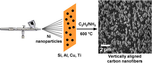 |
| This image illustrates how researchers use an airbrush to grow vertically aligned carbon nanofibers. (Image: Joseph Tracy.) |
| “It’s common to use nickel nanoparticles as catalysts to grow carbon nanofibers, and we were able to coat metal substrates with nickel nanoparticles using an airbrush,” says Dr. Joseph Tracy, an associate professor of materials science and engineering at NC State and senior author of the paper. “Airbrushing gives us a fairly uniform coating of the substrate and it can be applied to a large area at room temperature in a short period of time.” |
| After applying the nickel nanoparticles, the researchers airbrushed the substrate with a layer of silicon powder and heated the coated substrate to 600 degrees Celsius in a reactor filled with acetylene and ammonia gas. In the reactor, carbon nanofibers formed under the nickel nanoparticles and were held upright by a silicon-enriched coating. The finished product resembles a forest of nanofibers running perpendicular to the substrate. The researchers tested this technique successfully on aluminum, copper and titanium substrates. |
| “Growing carbon nanofibers on a metal substrate means the interface between the two materials is highly conductive, which makes the product more useful as an electrode material for use in a range of potential applications,” says Mehmet Sarac, a Ph.D. student at NC State and lead author of the paper. |
| Source: North Carolina State University |

