| Oct 28, 2013 |
Tin for faster chips
|
|
(Nanowerk News) To process and save data more and more quickly, to build even smaller and more powerful chips: these are the goals pursued by numerous research teams around the world. For some years now, one special material class has been at the heart of their efforts, so-called topological insulators. Within these, electrons automatically separate according to their respective spin orientation, entirely without the use of electric or magnetic fields.
|
|
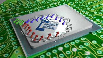
“This property is of far-reaching significance,” explains Professor Ralph Claessen from the Institute of Physics at the University of Würzburg: “If you apply electrical contacts to topological insulators, you can build circuits that transmit information coded with the spin orientation.” This new data transmission method is no longer based on the transport of electrical charges. It is therefore much faster and more reliable.
|
|
Why tin represents progress
|
|
Würzburg physicists have now, for the first time, succeeded in creating topological insulators made from tin, a simple and readily available material. “This makes production much easier because insulators like these have only ever been made from complex chemical compounds or hazardous materials,” says Claessen’s colleague Jörg Schäfer.
|
 |
| Topological insulator: in a layer of tin, electrons separate automatically according to the orientation of their spin, symbolized by arrows.
|
|
The physicists are presenting their findings in the journal Physical Review Letters ("Elemental Topological Insulator with Tunable Fermi Level: Strained α-Sn on InSb(001)"). They have achieved their success as part of an international collaboration with teams from Switzerland and the USA as well as from the Jülich Research Center. At Würzburg’s Institute of Physics, Professor Laurens Molenkamp also works with topological insulators, and successfully so: a few years ago, motivated by theoretical predictions, he became the first person to verify the unusual properties of this material class in a series of experiments.
|
|
How the topological insulator came about
|
|
In the new experiments under Ralph Claessen’s chairmanship and Jörg Schäfer’s leadership, thin layers of tin were vapor-deposited onto a semiconductor substrate extremely slowly. An orderly crystal lattice of tin atoms formed, identical to that of diamond.
|
|
“Experiments then revealed that this layer has the unusual properties we were looking for: the spins of the electrons are sorted into two directions with opposite magnetic needle orientation, and the two groups move in opposite directions,” says Schäfer. This was proven with spin-resolved photoemission.
|
|
“This has enabled us to show, for the very first time, that the phenomenon of automatic spin separation also exists in a simple, elementary crystal lattice,” enthuses Schäfer. As a result, he believes that the production of practical topological insulators is now tantalizingly close. The new experiments were underpinned by theoretical observations that Würzburg physics professor Werner Hanke made with colleagues in Jülich.
|
|
Next steps for the physicists
|
|
Since the spin separation in the tin lattice itself can now be reliably produced, the physicists next want to explore and optimize the conductive behavior of complete structures with electrical contacts.
|
|
Initial demonstrations of spin transport in layers with topological materials have already worked at temperatures well below freezing. So, for practical application, a number of technological issues still need to be clarified, including the realization of circuits that work without cooling. For this purpose, the Würzburg physicists are now working intensively together, pooling their expertise in material production and analysis.
|

