| Mar 13, 2014 |
Nanoscale 'earthquakes' move light along a nanowire |
| (Nanowerk News) Researchers at the MESA+ Institute for Nanotechnology at the University of Twente in collaboration with the Paul Drude Institute in Berlin have succeeded in moving light from one end of a semiconducting nanowire to the other by means of surface acoustic waves, a kind of nanoscale earthquakes. The results form an important milestone for the development of semiconductor devices which convert optical signals into electrical ones and vice versa, and bear direct relevance for quantum information processing. The findings were published in the journal Nanotechnology this week ("High-frequency acoustic charge transport in GaAs nanowires"). |
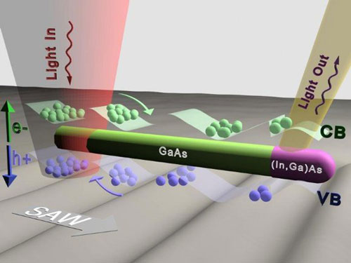 |
| GaAs nanowires with an indium-doped segment at one end were deposited on top of a LiNbO3 surface. LiNbO3 was used as a host material for SAWs because of its high piezoelectricity. A laser source was used to excite electron-hole pairs. These photo-generated electrons and holes are trapped at the spatially separated and piezoelectrically induced energy minima and maxima at the conduction band (CB) and valance band (VB) edges, respectively. These trapped carriers are then transported by the SAW with acoustic velocity to the (In,Ga)As region, where they recombine in quantum-dot-like centers. |
| Light is a very suitable medium to transfer information reliably over large distances, for example by glass fibers. On the other hand, information processing is more conveniently done electronically, taking advantage of all miniaturization and integration realized in semiconductors. Optoelectronic devices, which act as optical-to-electrical or electrical-to-optical transducers, are very much sought after as they connect both technologies. |
| What the researchers in Twente and Berlin have realized is actually an acousto-optoelectronic device, invoking next to optical and electrical signals, also acoustic ones. Laser light is focused on one end of a semiconductor (gallium arsenide) nanowire, where it excites electrons in the conduction band (CB), leaving holes in the valence band (VB). Both electrons and holes are picked up by a surface acoustic wave (SAW) that is produced at large distance from the wire on the same substrate. The SAW transports the electron-hole pairs efficiently along the nanowire. At the end of the nanowire the electrons and holes are forced to recombine, thereby producing light again. As the SAW travels about 100,000 times slower than light, manipulation can be done much more easily. |
| The technology developed at MESA+ and the PDI allows that this can be all done at very high frequencies (over 1 GHz) and at the nanoscale. This opens up the way for applying this kind of devices for quantum information processing as well. |
| Source: >University of Twente |

