| Posted: May 16, 2011 |
Researchers map out the switching location of a memristor |
| (Nanowerk Spotlight) Recent research suggests that memristor devices are capable of emulating the biological synapses of the brain with properly designed CMOS neuron components. A memristor is a two-terminal electronic device whose conductance can be precisely modulated by charge or flux through it. It has the special property that its resistance can be programmed (resistor) and subsequently remains stored (memory). In previous work, researchers have demonstrated that a memristor can connect conventional circuits and support a process that is the basis for memory and learning in biological systems (read more: "Nanotechnology's road to artificial brains"). |
| It is thought memristors – with the ability to 'remember' the total electronic charge that passes through them – will be of greatest benefit when they can act like synapses within electronic circuits, mimicking the complex network of neurons present in the brain, enabling our own ability to perceive, think and remember. Indeed, mimicking the brain's synapses could lead to a wide range of novel applications, including semi-autonomous robots, if complex networks of neurons can be reproduced in an artificial system. |
| Last year, researchers from HP Labs in California discovered that the memristor has more capabilities than was previously thought. In addition to being useful in storage devices, the memristor can perform logic, enabling computation to one day be performed in chips where data is stored, rather than on a specialized central processing unit. |
| Memristors have several attractive features that make them compelling for computer scientists: They require less energy to operate and are faster than present solid-state storage technologies such as flash memory, and they can store at least twice as much data in the same area. Memristors are virtually immune from radiation, which can disrupt transistor-based technologies – making them an attractive way to enable ever smaller but ever more powerful devices. Also, memristors can enable computers that turn on and off like a light switch. |
| Here, R. Stanley Williams, whose team discovered the memristor gives us a quick whiteboard talk about how the device works: |
| Stanley's team at Hewlett Packard, together with researchers at the University of California, Santa Barbara, have analyzed in unprecedented detail the physical and chemical properties of an electronic device that computer engineers hope will transform computing. |
| Reporting their findings in today's (May 16, 2011) online edition of Nanotechnology ("The switching location of a bipolar memristor: chemical, thermal and structural mapping"), the team correlate device electrical characteristics with local atomic structure, chemistry and temperature. We resolved a single conducting channel that is made up of a reduced phase of the as-deposited titanium oxide. |
| Memristors have a very simple structure – often just a thin film made of titanium dioxide between two metal electrodes. The team fabricated their memristive devices with a bottom electrode of chromium (5 nm)/platinum (18 nm), a top electrode of platinum (30 nm) and a switching layer of titanium dioxide (25 nm). The stack is fabricated atop a thin 20 nm silicon nitride window. |
| To map out the nanoscale physical and chemical properties of a memristor, the team used the scanning transmission x-ray microscope (STXM) at the Advanced Light Source. They used the highly focused x-rays to locate and image the approximately one hundred nanometer wide channel where the switching of resistance takes place, which was then fed into a mathematical model of how the memristor heats up during switching. |
| By sweeping the incident x-ray energy and measuring the fine structure of the titanium absorption spectrum, different material states – amorphous, anatase and a partially reduced sub-oxide – of the titanium oxide layer buried within the electrodes can be identified in a nondestructive manner. |
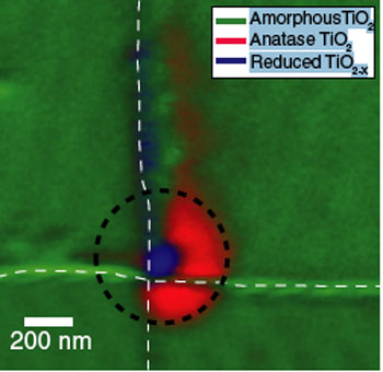 |
| Higher resolution scan of the bottom left corner of the junction with a spatial mapping of the three observed phases of titanium oxide present. The color mapping of these regions is derived from the Ti L2,3 x-ray absorption image stack using singular value decomposition procedures. A circle identifies the expected heated region surrounding the conductive channel (Reprinted with permission from IOP Publishing) |
| The researchers say that the heating pattern observed around the sub-oxide conductive channel (see above figure) provides a unique opportunity to better understand the ON/OFF switching in the bipolar operating mode of titanium dioxide devices. |
| "An important observation is the half-circle shape of the heated region. The anatase phase is only observed to be present above the bottom electrode, while one might expect the Joule heating from the sub-oxide channel to uniformly heat a circular pattern around the channel (dashed circle)." |
| The team believes that this semicircle pattern developed because of the specific location of the channel gap and therefore identifies the location at which ON/OFF switching occurred. They conclude: |
| "By comparing the semicircular shape and orientation of the observed anatase in the device with finite element simulations of the temperature profile caused by Joule heating, we deduced that the heating source was adjacent to the bottom electrode during switching." |
| "We now have a direct picture for the thermal profile that is highly localized around this channel during electrical operation, and is likely to play a large role in accelerating the physics driving the memristive behavior" says John Paul Strachan of the nanoElectronics Research Group at Hewlett-Packard Labs. |
 By
Michael
Berger
– Michael is author of four books by the Royal Society of Chemistry:
Nano-Society: Pushing the Boundaries of Technology (2009),
Nanotechnology: The Future is Tiny (2016),
Nanoengineering: The Skills and Tools Making Technology Invisible (2019), and
Waste not! How Nanotechnologies Can Increase Efficiencies Throughout Society (2025)
Copyright ©
Nanowerk LLC
By
Michael
Berger
– Michael is author of four books by the Royal Society of Chemistry:
Nano-Society: Pushing the Boundaries of Technology (2009),
Nanotechnology: The Future is Tiny (2016),
Nanoengineering: The Skills and Tools Making Technology Invisible (2019), and
Waste not! How Nanotechnologies Can Increase Efficiencies Throughout Society (2025)
Copyright ©
Nanowerk LLC
|

Become a Spotlight guest author! Join our large and growing group of guest contributors. Have you just published a scientific paper or have other exciting developments to share with the nanotechnology community? Here is how to publish on nanowerk.com. |
